


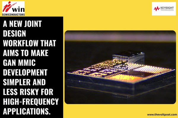
Keysight and WIN Semiconductors have launched a new joint design workflow that aims to make GaN MMIC development simpler and less risky for high-frequency applications. The idea is to help chip designers move more efficiently from simulation to fabrication while improving the odds of a successful first tapeout.
The workflow combines on-chip multi-domain simulation, 3D layout verification and off-chip evaluation board design in one environment. By bringing these steps together, the companies say engineers can evaluate chip, package and board performance as a whole before sending the design to the foundry.
This becomes important because a failed tapeout can be costly, both in time and money, and often means going back for another round of fabrication. This new flow is designed to reduce that risk by streamlining the simulation, optimization and verification steps that usually happen before production.
The solution is aimed at developers working on GaN MMICs for 5G base stations, Wi-Fi access points, satellite payloads and defense radar systems. In all of these areas, performance, reliability and speed to market are especially important.
At the center of the workflow is WIN Semiconductors’ NP 120P GaN Process Design Kit, which provides the process models and layout rules used within Keysight Advanced Design System and RF Circuit Simulation Professional. That integration helps create a smoother path from early design work to physical validation.
 For Keysight, the collaboration strengthens its position as a partner to RF and semiconductor teams looking to shorten development cycles and lower fabrication risk. For WIN Semiconductors, it expands the value of its GaN process technology by giving customers a better path toward successful tapeout.
