



The Centre for Advanced Studies in Electronics Science and Technology (CASEST) at the School of Physics, University of Hyderabad, has concluded two intensive three-week internship programmes that push beyond the usual theory-front format. From July 1-21, 2026, students were immersed in semiconductor microfabrication and VLSI design in a way that closely mirrors real industry workflows.
Chips Embedded in Certificates
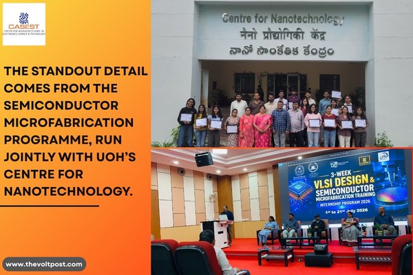
The standout detail comes from the Semiconductor Microfabrication programme, run jointly with UoH’s Centre for Nanotechnology.
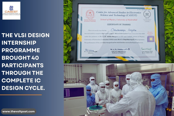
Each participant designed, fabricated, tested, and characterized a Thin Film Transistor (TFT) using the university’s cleanroom and microfabrication facilities. Instead of leaving with a conventional certificate, students received completion documents with their actual fabricated TFT embedded into them, turning a routine credential into a physical, lasting record of hands?on achievement.
The microfabrication track took students through the full device pipeline, wafer preparation, oxidation, photolithography, thin?film deposition, diffusion, etching, and metallization, giving them a start?to?finish view of how real devices are built on the fab floor.
Design to Fab: Twin Internship Tracks
Running in parallel, the VLSI Design Internship Programme brought 40 participants through the complete IC design cycle. Students worked through digital and analog IC design, Verilog HDL, RTL design, functional verification, logic synthesis, static timing analysis, physical design, and analog/mixed?signal layout.
Crucially, they did this on industry?standard EDA tools made accessible under the Chip2Startup (C2S) programme, part of India’s drive to democratize chip design capabilities across campuses.
Together, the microfabrication and VLSI tracks show what “from design to device” looks like in practice: one stream focused on circuits and layout, the other on turning those concepts into physical devices and process flows.
Industry Leaders Endorse India’s Chip Talent Pipeline
The programmes closed with a valedictory ceremony that placed the internships in the wider context of India’s semiconductor build-out.
Dr. Santosh Yachareni, Senior Director, Silicon Design Engineering at AMD India, served as Guest of Honour and spoke about the expanding opportunities as fabs, design centres, and validation teams grow across the country.
Prof. Samrat Sabat, Head of CASEST and Director R&D, highlighted the role of coordinators Dr. Anjali Priya and Dr. LD Varma Sangani in executing the programmes. Prof. Suresh P K (Dean, School of Physics) and Prof. J. Anuradha (Vice?Chancellor i/c) underlined how experiential, lab-led training of this kind is essential to building a skilled semiconductor workforce aligned with India’s national semiconductor mission.
Part of a Larger Skilling Wave
The UoH initiative fits into a broader national effort to make semiconductor education both hands?on and industry?aligned. Under Chips to Startup (C2S) and India Semiconductor Mission 2.0, advanced EDA tools and access to fabrication infrastructure are being extended to more institutes, so students train on the same workflows and toolchains used in industry.
Similar efforts such as IISc’s India Semiconductor Workforce Development Programme and fellowship?backed internships at institutions like BITS Pilani, Hyderabad are building device?level and process?level skills through cleanroom and lab exposure.
In that context, CASEST’s decision to embed each student’s own TFT into their certificate is both symbolic and practical, it compresses the entire “design to device” journey into something tangible that students can show, reflect on, and build upon.
 From Campus Labs to Fab-Ready Talent
For India’s proposed fabs and expanding design houses, the limiting factor is increasingly trained talent rather than just capital or equipment.
Programmes like those at the University of Hyderabad demonstrate a campus-level blueprint, combining microfabrication lines, VLSI design labs, and industry mentorship to create internship cohorts that have already handled wafers, run real flows, and understood the constraints of fabrication before entering the job market.
As more universities align with national programmes and industry partners, “from design to device” is likely to move from slogan to standard practice in semiconductor education across India. For this latest CASEST batch, that progression is already etched, literally into the certificates they carried home, with a self?fabricated TFT as proof of what they built and learned.