



As wearables like smart rings, fitness bands, and VR glasses pack in more features, finding room on the circuit board is becoming a major challenge for hardware designers. To help ease the compact form factor, Renesas Electronics has rolled out the SLG46801, stated officially by the company as the industry’s smallest configurable mixed-signal device in its GreenPAK lineup.

Measuring a microscopic 1.155 by 1.155 millimeters in its 9-ball WLCSP package, this multi-time programmable chip is designed to do the heavy lifting of several components at once. By rolling commonly used analog, timing, and logic functions into one tiny footprint, it acts as the perfect sidekick to a main microcontroller, freeing up valuable board space and driving down the overall bill of materials.
Under the hood, the SLG46801 packs a surprisingly robust feature set. It integrates two high-speed analog comparators, configurable lookup tables, counters, delays, and both 10 kHz and 25 MHz oscillators. It also features voltage-tolerant GPIOs and an I²C-compatible serial interface, handling everything from sensing and system housekeeping to “glue-logic” across smart home systems, IoT sensors, and industrial controls.
Fixing Bugs After Shipping Perhaps the most significant advantage for developers is the chip’s multi-time programmable, non-volatile memory.
Because it can be configured in-system via the I²C interface, engineers can push bug fixes, adjust configurations, or roll out product upgrades even after the device has been built into a consumer’s gadget. This on-the-fly adaptability can drastically reduce the need for costly hardware redesigns.
It’s also highly adaptable on a hardware level. The chip operates across a 1.71 V to 5.5 V supply range, the widest available among MTP GreenPAK devices.
When pin availability is a challenge, the GPIO pins can be dynamically repurposed for the I²C interface. For added security, optional CRC-8 and read-back protection ensure that the configurations remain robust and controlled.
Balancing Size and Capability While the 9-ball WLCSP is built for absolute space-saving, Renesas is also offering the SLG46801 in a slightly larger 12-lead STQFN package (1.6 × 1.6 × 0.55 mm).
This gives manufacturers the flexibility to trade a tiny bit of board space for extra GPIO availability, depending on their industrial design needs. Both options boast one of the lowest costs per GPIO in the entire GreenPAK family.
Renesas has already shipped more than four billion GreenPAK devices globally, cementing its footprint in the mixed-signal space.
Keeping with the ecosystem’s user-friendly approach, engineers can skip the complex firmware coding entirely. The new chip can be completely configured using the free, drag-and-drop Renesas Go Configure™ Software Hub, making custom hardware development faster and far less of a headache.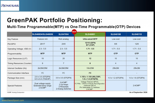
Leadership Comment
“Designers are being asked to integrate more functionality into increasingly compact products without increasing system cost or development effort, while also reducing power consumption.” said Jason Kim, Vice President and General Manager of the Core Analog Division at Renesas. “The SLG46801 expands our GreenPAK portfolio with an ultra-compact WLCSP option and flexible in-system configurability, helping customers create smaller, more feature-rich products and implement updates even after deployment.”
Availability
The SLG46801 in the STQFN package is sampling now, with the WLCSP package available at mass production planned for November 2026.
Renesas Go Configure Software Hub is available for programing, emulation and simulation.
More information is available at https://www.renesas.com/products/slg46801