



The two-decade reign of the 300mm silicon wafer might be coming to an abrupt end, and Japan is positioning itself to own the next era of semiconductor manufacturing.
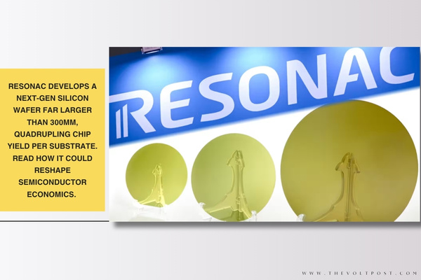
According to a new report, Resonac Holdings has engineered a next-generation silicon wafer significantly larger than today’s industry standard. The breakthrough substrate is reportedly capable of yielding roughly four times as many chips per wafer, a monumental leap in die output that could fundamentally rewrite semiconductor economics.
But before fabs can reap the benefits of quadrupled output, the industry faces a massive structural bottleneck and that is the equipment ecosystem.
Historically, migrating to a larger wafer format demands a ground-up re-engineering of the entire fab floor. Everything from furnaces and polishers to robotic handlers and lithography stages must be redesigned around the new dimensions.
The industry notoriously stonewalled similar capital investments during the stalled 450mm push years ago, with equipment manufacturers refusing to fund tool development without ironclad volume commitments from fabs. Resonac’s new format will inevitably face the exact same standoff.
If they can break that deadlock, the commercial upside is staggering. Wafer diameter remains one of the last true levers to aggressively drive down per-chip costs.
Because the baseline processing costs for deposition, lithography, and etching remain relatively static regardless of die count, quadrupling the yield spreads those expenses across a much higher volume, translating directly into massive gross margin gains for high-volume products.
A Larger Panel-Scale Format Perfectly Accommodates This Shift
This expanded silicon real estate also arrives at the perfect time for the advanced packaging boom.
As traditional logic scaling plateaus, fabs are increasingly building systems by stacking and stitching dies side-by-side on massive interposers.
A larger panel-scale format perfectly accommodates this shift, allowing multiple reticle-sized dies or entire packaged modules to run in a single process flow.
Owning the IP For a Next-Gen Substrate
For Resonac which was born from the merger of Showa Denko and Hitachi Chemical’s materials arms, this breakthrough is a highly calculated defensive maneuver.
Owning the IP for a next-generation substrate provides a distinct competitive moat against heavyweights like Shin-Etsu Handotai, SUMCO, and Taiwan’s GlobalWafers, allowing them to escape the heavily commoditized 300mm price wars.
The move also carries immense strategic weight in Tokyo. As global chipmaking capacity rapidly consolidates across the U.S., Taiwan, and South Korea, the Japanese government has been aggressively subsidizing its domestic supply chain. Because wafer substrates sit at the absolute top of that chain, a homegrown leap in format size firmly cements Japan’s non-replaceable role in the global market.
For now, Resonac’s fourfold yield figure remains a development-stage capability. Nikkei’s report leaves out exact target dimensions, commercial timelines, or active customer evaluations.