



IZMO Limited’s semiconductor subsidiary, izmo Microsystems, has developed a high-frequency RF QFN Package designed for semiconductor devices operating at frequencies of up to 40 GHz.
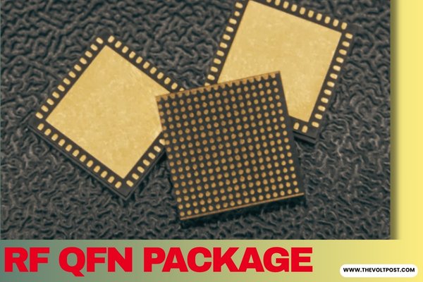
Designed, developed and manufactured entirely in India, the 40 GHz RF QFN Package has been developed for a customer working on high-frequency RF modules for defence and secure wireless communication applications.
Following successful assembly and electrical validation, izmo Microsystems has now started production shipments, with manufacturing processes in place to support further scale-up.
The development marks a step forward in the company’s RF and microwave semiconductor packaging capabilities and highlights its ability to develop application-specific packaging solutions and take them through to volume manufacturing.
Package architecture targets high-frequency performance
As operating frequencies move higher into the microwave range, conventional molded and open-cavity QFN packages can encounter performance challenges. Package parasitics can increasingly influence device performance, making package design a critical part of the overall RF solution.
To address these challenges, izmo Microsystems developed a proprietary package architecture featuring optimized trace geometry and die positioning. The design achieves wire bond lengths of approximately 0.3 mm and incorporates a precision air cavity around the die.
According to the company, the architecture is designed to reduce parasitic effects and support reliable semiconductor device operation at frequencies of up to 40 GHz.
Target applications include radar and secure communications
The new packaging capability is aimed at high-frequency applications where RF performance and reliability are critical. Potential applications include radar, electronic warfare, secure communications, aerospace, satellite communications and advanced wireless systems.
The development also comes as India places greater emphasis on domestic semiconductor and defence electronics capabilities. Growing defence requirements, increased focus on indigenous procurement and the strategic importance of secure communications are driving demand for advanced electronics technologies that can be developed and manufactured within the country.
For strategic applications, building critical RF packaging capabilities domestically can also help strengthen supply-chain resilience and reduce dependence on overseas packaging technologies.
Advanced packaging gains importance in India’s semiconductor push
The development comes against the backdrop of India’s broader efforts to strengthen its semiconductor manufacturing ecosystem. The Government of India has approved Semicon 2.0 with an outlay of ?1,27,500 crore, aimed at further developing the country’s semiconductor design and manufacturing capabilities.
Advanced packaging is expected to play an increasingly important role in this ecosystem, particularly as India expands its ATMP and OSAT capabilities and moves toward more sophisticated semiconductor manufacturing and packaging technologies.
For izmo Microsystems, the new RF QFN package adds to its capabilities across package and process development, prototyping, qualification and manufacturing, with a focus on advanced and high-reliability semiconductor applications.
The ability to develop and manufacture a 40 GHz RF package entirely in India could be particularly significant for defence, aerospace and secure communications applications, where performance, reliability and supply-chain security are critical considerations.
Leadership Comment
Dinanath Soni, Director, izmo Microsystems Pvt. Ltd., said:
“High frequency RF devices place very demanding requirements on semiconductor packaging, and at 40 GHz the package has to be engineered as an integral part of the RF system.
 We developed this package around the specific electrical and application requirements of the device and have taken it through design, fabrication, assembly and validation into production. Production shipments have now commenced, and we have the manufacturing capability to scale as requirements grow.
We see significant opportunities for advanced RF packaging in defence, secure communications, aerospace and other high frequency applications as India builds deeper domestic capabilities in strategic electronics and semiconductor manufacturing. The increased focus on advanced packaging under Semicon 2.0 should provide further impetus to the development of this ecosystem in India.”
To Know More: CLICK HERE