


Samsung aims to reclaim the high ground in AI memory by unveiling a new architecture that stacks high-bandwidth memory directly on top of AI accelerators. The system, called zHBM, is designed to deliver roughly eight times the performance of next-generation HBM5 while packing in more than 10 times the memory density, thanks to advanced wafer-bonding technology.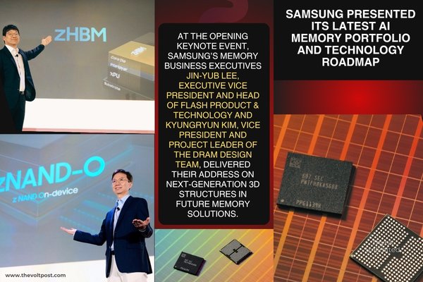
zHBM: stacking memory on top of AI accelerators
Unlike today’s HBM, which sits beside the GPU or AI chip, zHBM places the memory vertically above the accelerator to slash the distance data has to travel.
Samsung says this arrangement boosts bandwidth and energy efficiency, tripling energy efficiency and cutting thermal resistance by more than half compared to conventional HBM5. The company is positioning zHBM as the cornerstone of an end-to-end AI infrastructure stack, aiming to lock in data center customers ahead of rivals SK Hynix and Micron.
Samsung has not given a firm timeline for zHBM or HBM5, but it does plan to ramp HBM4 production in the second half of 2026 as it chases Nvidia and other large AI chip buyers.
V10 BV-NAND: 400+ layers and a new bonding approach
On the storage side, Samsung introduced the industry’s first V10 BV-NAND, a V-NAND architecture built around a new wafer-bonding design with more than 400 layers.
By separating the memory array from the peripheral logic and then bonding the wafers together, Samsung says it can increase storage density by about 58% over its previous V9 generation while improving read, write, and I/O speeds.
The move is a clear signal that Samsung wants to lead not just in HBM, but across the full memory and storage stack for AI workloads.
zNAND-O and the broader AI roadmap
Samsung also showed zNAND-O, a next-generation NAND solution optimized for real-time, data-intensive AI applications, with four- and eight-layer versions in development.
Alongside these hardware reveals, the company displayed a roadmap that includes next-generation processing-in-memory chips and high-capacity enterprise storage, underscoring its push to become a one-stop supplier for AI infrastructure.
In a market now approaching $1 trillion, the stakes are simple, whoever ships the most compelling AI memory architecture first stands to win the biggest data center contracts.
Samsung’s zHBM and V10 BV-NAND are its answer to SK Hynix’s early lead and Micron’s aggressive push betting that vertical stacking and wafer bonding will define the next era of AI memory.
To Know More: CLICK HERE