


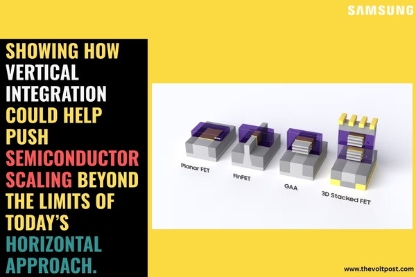
Samsung is taking another step toward the future of transistor scaling with a new 3D Stacked FET design that moves logic devices into the third dimension. The company says the research demonstrates a 42 nm gate-pitch structure using triple-stacked nanosheet channels, showing how vertical integration could help push semiconductor scaling beyond the limits of today’s horizontal approach.
Samsung Semiconductor’s Research Center presented the work at the 2026 VLSI Symposium. The paper, titled “First Demonstration of 3D Stacked FETs at Gate Pitch of 42 nm Featuring Triple Stacked Nanosheet Channels for Advanced Logic Applications,” drew strong interest for its technical importance and was highlighted as one of the event’s standout contributions.
At its core, the idea behind the 3D Stacked FET is simple but ambitious. Instead of placing n-type and p-type transistors side by side, Samsung stacks them vertically. That could improve density significantly without relying only on shrinking devices further across the chip.
The approach builds on gate-all-around technology, one of the most advanced transistor architectures in use today. Samsung’s latest design takes that concept further by using nanosheet channels in a vertically integrated structure, offering a new path for logic scaling as the industry continues to face growing physical and manufacturing challenges.
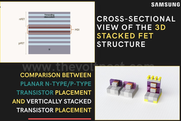
The company says the work tackles three of the biggest hurdles in stacked transistor design, preserving drive current, growing high-quality stacked channel layers, and keeping the upper and lower devices properly isolated. To address these issues, the company combined triple-stacked nanosheet channels with optimized epitaxial growth and middle dielectric isolation.
One of the most important details is the 42 nm gate pitch, which Samsung describes as a meaningful step toward practical 3D stacked logic devices. Smaller gate pitches can improve density, but they also make fabrication more difficult, which makes this result notable from both a research and manufacturing standpoint.
 The company also reported strong current-control behavior and wafer-wide uniformity, suggesting the design has real potential beyond the lab. That makes the breakthrough more than just a concept and points to a future where vertical transistor architectures could become central to chip design.
As traditional scaling becomes harder to maintain, the industry is looking for new ways to improve performance, density, and efficiency. The company’s 3D Stacked FET research suggests the next big leap may come not from making transistors flatter and smaller, but from stacking them more intelligently.
