




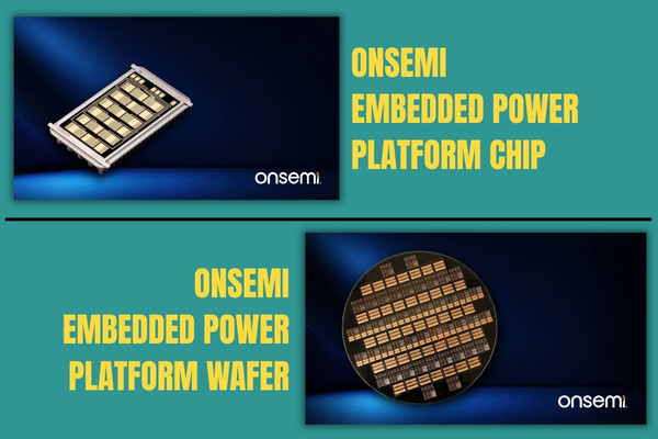
Engineers need to pack more electricity into increasingly shrinking spaces while somehow keeping heat, costs, and development times under control. Lately, onsemi unveiled a radically different approach to solving this bottleneck with its new Embedded Power Platform (EPP).
As artificial intelligence, electric vehicles, and industrial automation push the limits of modern infrastructure, they are all colliding with the same massive roadblock and that is power constraints.
Engineers need to pack more electricity into increasingly shrinking spaces while somehow keeping heat, costs, and development times under control. Lately, onsemi unveiled a radically different approach to solving this bottleneck with its new Embedded Power Platform (EPP).
Instead of relying on the traditional method, where a chip’s passive housing is designed separately from its electrical and thermal systems, EPP flips the script. It uses the silicon wafer itself as the foundational package, turning it into an active contributor to the system’s overall performance.
Automakers Are Already on Board
The industry is moving fast to test the waters. Subaru Corporation has already stepped up as an early engagement partner, collaborating with onsemi to see how EPP can power its next generation of electrified vehicles.
Through the partnership, Subaru gets early access to engineering samples and simulation models to figure out how to squeeze more performance out of their cars while trimming down development time.
Breaking the Engineering Bottleneck
Historically, building power systems has been a clunky, sequential process. Engineers would tackle power electronics, mechanical design, and thermal management as isolated steps.
A tweak in one department often caused a headache in another, leading to endless revisions, late-stage redesigns, and delayed product launches.
EPP scraps that outdated model. By leveraging onsemi’s standard 12-inch silicon wafer manufacturing, the platform allows engineers to seamlessly combine silicon, silicon carbide (SiC), and gallium nitride (GaN) technologies right at the wafer level.
Because FETs, drivers, and controllers are embedded together from day one, teams can co-design and optimize everything, electrical, mechanical, and thermal simultaneously.
The resulting performance leap is massive. According to onsemi, moving to this unified architecture allows customers to:
- Boost power density by 3x to 5x, depending on the application.
- Slash development cycles down to as little as four months.
- Dramatically improve heat dissipation and overall thermal performance.
- Cut electrical losses and enable much higher switching frequencies.
- Scale a single architecture across different power levels and vehicle classes.
Real-World Impact
AI and EVs In the real world, this translates to smaller, cooler, and vastly more efficient systems.
Take AI infrastructure. As server racks draw increasingly massive amounts of power, the hardware needed to convert and protect that energy is eating up valuable physical space and cooling capacity, space that should be used for computing.
By using the entire EPP footprint to conduct heat and reducing packaging overhead, early designs of an EPP-based solid-state circuit breaker came out 50% smaller and 20% cooler than current standard designs.
The impact on electric vehicles is equally stark. EV traction inverters are notorious for their thermal limits and efficiency losses. By moving to EPP, automakers can hit up to 4x higher power density with 15% fewer power losses. Even better, the scalable design means a car company can use the exact same inverter platform for both a budget-friendly commuter EV and a high-end luxury model, saving millions in R&D and manufacturing costs.
Computing power alone isn’t going to solve the infrastructure hurdles of the AI and electrification era. As energy delivery becomes the defining constraint of the next decade, onsemi’s decision to turn the wafer itself into the package might just be the foundation the industry has been looking for.
Leadership Comment
 “For decades, the semiconductor and the package have been treated as separate technologies. EPP changes that by making the silicon itself part of the system architecture,” said Hassane El-Khoury, President and CEO of onsemi. “EPP brings together advanced semiconductor technologies, manufacturing and system-level optimization into a common architecture that can evolve alongside future innovations. This approach can redefine how power systems are built and create a new foundation for AI infrastructure, electrification and automation.”
Availability
EPP is expected to begin sampling in 2026 with strategic customers and ecosystem participants across automotive and AI applications.
To Know More: CLICK HERE