


In September 2025, Dai Nippon Printing plans to open its first research and development (R&D) center abroad in the Netherlands. The High Tech Campus Eindhoven (HTCE) will house the new R&D Center, which will accelerate innovation and support global R&D.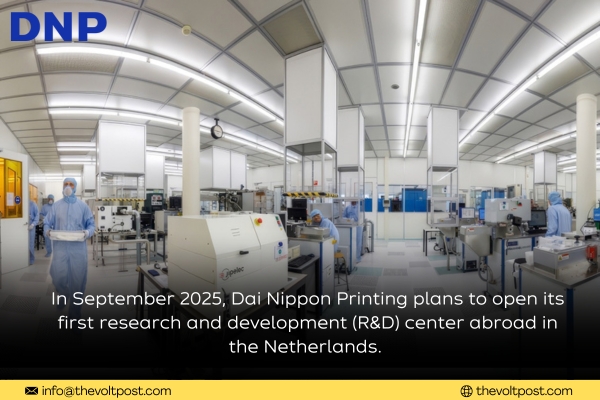
More than 12,500 academics, engineers, and entrepreneurs collaborate with about 300 businesses and research institutions at HTCE, one of Europe’s top innovation hubs, to create cutting-edge products and technology.
Dai’ initial project will advance research and development in Co-Packaged Optics, which combines electronic and optical communication technologies to provide high information processing performance. Co-packaged optics is gaining popularity as a semiconductor technology of the future.
A collaborative research and development agreement on co-packaged optics was signed by Dai and the Netherlands Organization for Applied Scientific Research (TNO) in July 2025. The Photonic Integration Technology Centre (PITC), a campus-based research institution that links fundamental studies to the mass manufacturing of photonic chips (optical IC chips), will support these initiatives.
DNP will collaborate with PITC and other HTCE-based organizations for three years to expedite the development of package components for Co-Packaged Optics. The objective is to form new alliances and acquire state-of-the-art technologies, such as precision patterning technology for optical materials associated with Co-Packaged Optics.
Co-Packaged Optics technology exhibits a high information processing performance, low power consumption, and energy savings, and is expected to be deployed in next-generation semiconductors.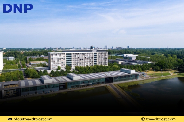
Through the new R&D base in the Netherlands, DNP will gain access to technologies and Co-Packaged Optics-related R&D networks, further accelerating the development of package components for Co-Packaged Optics.
