


Heat and power limits are becoming the biggest hiccups for next-gen AI and 6G chip development. But a fresh partnership between Purdue University and Taiwan’s GeChi Compound Semiconductor (GCCS) might just be the breakthrough the industry’s been chasing.
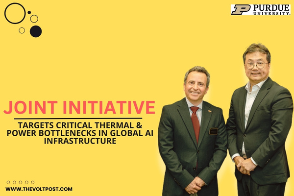
The two just locked in a 5-year deal focused on silicon carbide (SiC) R&D, plus a workforce program that actually connects classroom learning with real factory floors.
Why Silicon Carbide Is Suddenly Everyone’s Business
Silicon carbide isn’t your average semiconductor. It’s a third-gen material that leaves traditional silicon in the dust when it comes to performance:
SiC tackles the heat and power problems that choke high-performance systems. Where does that matter most?
- AI data centers: Chips gobbling massive power need better heat management and here SiC delivers.
- 6G networks: Next-gen connectivity demands material efficiency only SiC can provide.
- Electric vehicles: Smaller, leaner power conversion systems mean longer range and faster charging.
What Makes This Partnership Different?
Most semiconductor partnerships are about building more factories. This one’s different it’s about fixing the process itself.
The collaboration zeroed in on three tough problems:
- Crystal defects: Joint research will hunt down structural flaws in SiC crystal lattices
- Material growth: Tighter control over how SiC crystals form means fewer wastes and higher yields
- Bigger wafers: Pushing fast from 6-inch to 8-inch and 12-inch wafers for serious production gains
Kuan-Ming Hsiung, GCCS’s chairman, said:
“By combining our manufacturing capabilities with America’s top academic institution, we are decisively moving to keep the silicon carbide supply chain domestic.”
It will not just be better materials but about building flexible, high-yield manufacturing right in the U.S. and that’s a national security focus.
GCCS Brings Taiwan’s Edge to American Soil
GCCS knows SiC crystal growth inside and out. They’re bringing Taiwan’s semiconductor engineering know-how to scalable U.S. manufacturing infrastructure.
This partnership signals a bigger shift as third-gen semiconductor production is moving back home to the U.S., with large-wafer fabrication at the center.
Purdue‘s Semiconductor Initiatives
- Launched America’s first full-stack Semiconductor Degrees Program on-campus, online, apprenticeships
- Got $100 million to upgrade facilities, including the famous Birck Nanotechnology Center
- Deep ties with IBM, Intel, SkyWater Technologies, and MediaTek
- Built a $1.8B fab on campus with SkyWater
