


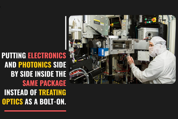
MIT researchers are betting that the next leap in performance will come from putting electronics and photonics side by side inside the same package instead of treating optics as a bolt-on. Through the FUTUR-IC program they have introduced new optical coupling devices that behave like “optical bumps,” giving photonic chips the kind of repeatable, production ready interconnects that metal solder bumps already provide for electronic dies.
Rising data bottleneck
Today’s accelerators burn a surprising amount of power just moving data between compute dies, high bandwidth memory stacks, and network interfaces, and those electrical links only get hotter and less efficient as line rates climb.
Co?packaged optics attacks that bottleneck by pushing high speed signals into light as early as possible inside the package, shortening the electrical runs and cutting losses compared with pluggable optical modules that sit farther away on the board.
Inside the FUTUR-IC program
Backed by the US National Science Foundation’s Convergence Accelerator, FUTUR-IC brings together materials scientists, photonics specialists, packaging engineers, and industry partners around a single question, how to build microchip systems that move vastly more data without burning through more energy and capital equipment.
The team is aiming to lift data movement from today’s hundreds of terabits per second to beyond one petabit per second while keeping the manufacturing flow compatible with established foundry and packaging lines.
Optical bumps for photonic chips
The latest results centre on three optical couplers that route light between chips and layers inside a package, giving designers a menu of options much like the different solder bump styles they already use in conventional electronics.
Two couplers, an evanescent design and a graded index device known as a GRIN coupler, came out of FUTUR-IC, while a third originated in a separate effort led by MIT materials science professor Juejun Hu.
Evanescent coupler focus
The evanescent coupler hands off light between stacked waveguides using overlapping optical fields, which relaxes alignment demands and makes it easier to assemble optical packages with passive alignment tools already familiar to high volume packaging lines.
Because it supports very dense integration, it can host large numbers of optical connections in tight spaces, a critical advantage for AI accelerators that need many high bandwidth links between logic, memory, and photonic engines.
 GRIN coupler advantages
The GRIN coupler changes the refractive index profile across the device to steer light between waveguides, trading some fabrication simplicity for broad wavelength compatibility.
That wider spectral window makes it a strong fit for systems that multiplex several colours of light inside a single optical package to grow capacity without adding more physical links.
Need for multiple coupler types
MIT engineers are clear that one coupler will not suit every package, and real products will likely mix several optical bump types to balance efficiency, cost, and density.
In practice, a packaging team might lean on evanescent couplers where tight integration and easier assembly matter most, and reserve GRIN couplers for sections of the system that need broad wavelength support and flexible routing for complex optical fabrics.
Manufacturing and supply chain impact
A hard constraint for FUTUR-IC has been manufacturability on existing tools in conventional electronics foundries and packaging houses, rather than demanding exotic new process flows.
By designing for passive alignment and familiar assembly steps, the team is trying to give chipmakers and outsourced assembly and test vendors a realistic path to add optical bumps alongside metal ones without blowing up their cost models or reliability playbooks.
Energy and sustainability stakes
MIT points out that microchips are linked to hundreds of megatons of lifetime carbon dioxide equivalent emissions, and that data centres could edge toward a tenth of global electricity use by 2030 if current trajectories hold.
FUTUR-IC’s guiding idea is simple, let electronics focus on computation and shift the heavy duty communication onto lower loss optical channels to help keep the sector’s energy footprint in check.
Earthster for lifecycle insight
To move beyond device physics and into real world impact, FUTUR-IC includes Earthster, a platform that lets companies run life cycle assessments across their product lines and quickly spot energy, materials, and carbon hot spots.
Suppliers can use Earthster’s visual outputs to see which process steps drive the biggest environmental load and prioritise redesigns or sourcing changes that deliver meaningful emissions cuts rather than incremental tweaks.
Workforce and ecosystem building
The program is also investing heavily in people, with online courses on semiconductor resource efficiency, gamified digital modules, summer academies, and hands?on bootcamps aimed at engineers who will have to make these technologies work in production.
For school students and general audiences, FUTUR-IC has produced TED?Ed style content that introduces microelectronics, photonics, and sustainability, reflecting the wider talent crunch around advanced packaging and integrated photonic systems.
Implications for data centres and edge systems
For hyperscale data centres, mature optical bump technology could make it far easier to co-package compute dies, memory tiles, and photonic engines in a single module tuned for bandwidth, latency, and power rather than just raw FLOPS.
At the edge, robots and vehicles that must process rich sensor data locally could lean on similar electronic photonic integration to move information inside the box more efficiently, freeing thermal and battery budget for sensing, actuation, and safety margin.
Can it be a game-changer for chip designers?
If these couplers make the jump from lab prototypes to high yield, high reliability building blocks, chip designers could start treating optical interconnects with the same confidence they reserve for solder bumps, routing light across dies and substrates as a standard resource instead of a bespoke feature.
That change would open new partitioning strategies in AI accelerators, networking silicon, and specialised compute platforms, with photonic tiles carrying the bulk data streams and electronic cores concentrating on logic, control, and orchestration.
To Know More About, CLICK HERE