


MIT Bengaluru, a constituent unit of Manipal Academy of Higher Education (MAHE), is taking a significant step toward strengthening India’s semiconductor talent pipeline. The institute is offering students rare, hands-on exposure to advanced chip fabrication environments and connecting them with global semiconductor ecosystems.

As India accelerates its push to become a global semiconductor and manufacturing hub, MIT Bengaluru is aligning its engineering education with industry needs through experiential and industry-integrated learning on advanced chip fabrication. The focus is on preparing students for real-world challenges in next-generation technologies.
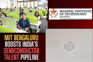
In a notable initiative, selected students from MIT Bengaluru recently completed nearly 120 hours of hands-on training at a specialized Class 100–10,000 cleanroom facility at CMTI.
During the program, students worked directly on semiconductor fabrication processes, including wafer cleaning, etching, deposition, lithography, characterization, integration, and dicing. They also successfully fabricated a 600-micron MOS (metal-oxide-semiconductor) capacitor, an opportunity that remains rare for undergraduate students in India.
This initiative highlights the institutions broader commitment to building expertise in emerging domains such as advanced chip fabrication, VLSI engineering, AI hardware, EV chip ecosystems, and advanced electronics manufacturing.
The program also reflects the institute’s growing engagement with Taiwan’s globally renowned semiconductor ecosystem, including institutions linked to TSMC, the world’s largest semiconductor manufacturer.
Through such collaborations, students gain exposure to advanced fabrication processes, chip design workflows, and evolving deep-tech industries, opening pathways to global semiconductor careers.
As India continues to expand its semiconductor ecosystem through new investments and international partnerships, MIT Bengaluru’s approach offers a forward-looking model for developing the next generation of engineers and innovators in this critical sector.
 Leadership Comments
Reflecting on the initiative, Prof. Madhu Veeraraghavan, Pro Vice-Chancellor, MAHE Bengaluru, said, “India’s semiconductor journey cannot be built on policy alone. It must be built on people, deep-tech innovations, advanced manufacturing capability, and globally relevant talent ecosystems. Institutions must move beyond conventional learning models and create opportunities that prepare students for emerging technology sectors of national importance. Initiatives like this reflect the kind of institution, industry, and international collaboration that will determine whether India’s semiconductor ambitions translate into real engineering capability.”
Dr. Iven Jose, Director, MIT Bengaluru, said, “Unlike conventional engineering programs that rely mainly on simulation-based learning, MIT Bengaluru emphasizes impact-based teaching, project-driven learning, and industry-integrated pedagogy. This initiative reflects our commitment to next-generation engineering education by enabling students to experience semiconductor fabrication environments, chip-processing workflows, and real-world semiconductor ecosystems firsthand.”
As India expands its semiconductor ecosystem through new investments and global partnerships, MIT Bengaluru’s initiative represents a forward-looking model for preparing the next generation of semiconductor engineers and innovators.
To Know More: CLICK HERE
