


Huawei has unveiled what it’s calling a chipmaking breakthrough, one that could help it narrow the gap with Taiwan Semiconductor Manufacturing Co. (TSMC), the world’s dominant foundry, known as Tau Scaling Law.

P.C. : Huawei
The Chinese tech giant says it has developed a design-driven approach that lets it push performance closer to the global frontier without depending on the ultra-advanced manufacturing tools its rivals rely on. That’s significant in an industry that long treated “smaller transistors” as the only credible path forward.
Today, there’s roughly a five-year lag between what TSMC can produce and what Huawei can deliver through its partnership with Semiconductor Manufacturing International Corp. (SMIC). Now, Huawei is betting on a new direction built around time?based scaling, which it’s calling the “Tau (?) Scaling Law.”
Rather than focus only on shrinking transistors geometrically, the company is trying to compress how long it takes for signals and data to travel through chips and systems. The logic is simple, shorter delays and denser layouts can deliver benefits similar to physically finer nodes, even when running on older equipment.
At the heart of this strategy lies “LogicFolding,” a new architecture Huawei plans to roll out in its upcoming Kirin smartphone chips later this year.
LogicFolding shortens the wiring paths inside the chip, lowers resistive-capacitive load, and increases transistor density all while working with existing or restricted manufacturing tools.
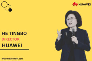
Huawei’s semiconductor chief, He Tingbo, has said the company expects its high-end chips to reach transistor density equivalent to a 1.4-nanometer process by 2031. If that actually plays out, it would start chipping away at TSMC’s lead and force a rethink of how the industry measures scaling progress.
Huawei isn’t claiming to overtake TSMC on volume or breadth any time soon. TSMC is already working with 2-nm-class technology and plans to mass?produce a 1.4-nm node around 2028.
But the company’s message is that it now has a structural workaround, a way to keep improving performance and density even as U.S. export controls constrain access to cutting-edge kit like ASML’s most advanced EUV lithography systems. That in turn could help pull more of China’s semiconductor value chain away from Western equipment and intellectual property.
For the broader market, Huawei’s move is less about matching TSMC’s fabs tomorrow and more about proving there may be alternative routes to advanced computing. If the Tau Scaling Law and LogicFolding live up to the promise, they could reshape how designers think about power, performance, and system-level optimization.
It has already known to have integrated this philosophy into more
than 380 chips it has designed and mass-produced over the past six years, covering smartphones, AI workloads, and infrastructure gear.
The company’s roadmap won’t erase the gap with TSMC in a single step, but it does suggest that the future of chips may depend as much on smart architecture and system-wide co-design as on the latest lithography node.
