


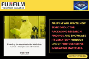
FUJIFILM Corporation announced it will unveil new semiconductor packaging research findings and showcase its ZEMATES™ product line of photosensitive insulating materials including PFAS-free PBO at the Electronic Components and Technology Conference 2026 (ECTC 2026), taking place May 26–29, 2026, in Orlando, Florida.

As part of the conference’s technical program, Fujifilm will present joint research results with imec, a top international research institute for nanoelectronics and advanced semiconductor technologies.
FUJIFILM Electronic Materials U.S.A., Inc., the company’s U.S.-based semiconductor materials subsidiary, will also exhibit at the conference (Booth #1003).
ECTC is the world’s largest international conference focused on semiconductor packaging technologies, drawing more than 2,500 scientists, engineers, and business leaders from across the global semiconductor ecosystem.
New Bonding and Interconnect Layer Process Research
Fujifilm’s technical presentations will zero in on bonding and interconnect formation technologies that enable further miniaturization of advanced packages, including 2.xD and 3D architectures and high-bandwidth memory (HBM).
- Sn (Tin) Damascene Process for Fine-Pitch Microbumps
Fujifilm and imec jointly developed a Sn damascene bonding process that pushes microbump miniaturization even further, expanding bonding solutions beyond hybrid bonding approaches. The presentation will cover lithography and polishing evaluation results using Fujifilm materials. - Damascene Interconnect Layer Process for 1.0 µm Line-and-Space
Working with imec, Fujifilm contributed to developing a damascene copper interconnect process capable of forming 1.0-micrometer line-and-space patterns. imec will deliver this presentation, with Fujifilm listed as a co-author.
ZEMATESTM & PFAS-Free PBO Development
The ZEMATES™ product lineup includes liquid-type polyimide for redistribution layers (RDL) and protective films, film-type polyimide for redistribution layers, and PBO (polybenzoxazole) for protective films.
These insulating layer materials serve semiconductor packaging processes spanning everything from power semiconductors to high-performance AI chips.
As regulatory and customer interest in PFAS-free materials grows, Fujifilm developed PFAS-free PBO formulations that don’t rely on PFAS-containing raw materials.
Leveraging Fujifilm’s decades-long expertise in molecular design, formulation, and analysis rooted in both photographic film technology and semiconductor materials development, the company achieved PFAS-free PBO materials while maintaining patterning performance and mechanical properties on par with conventional products.
Customer evaluations are currently underway at multiple sites, with commercialization targeted for 2026.
Exhibition Highlights
At booth #1003, FUJIFILM Electronic Materials U.S.A., Inc. will showcase a range of materials for advanced semiconductor packaging, including:
- Polybenzoxazole (PBO) dielectric insulating films, including newly developed PFAS-free formulations responding to rising demand
- Polyimide materials in both liquid and film formats
- Thermal management materials like heat dissipation sheets
- CMP slurries and back-end process materials used in advanced semiconductor manufacturing
 Leadership Comment
“Fujifilm’s new PFAS-free PBO product shows Fujifilm’s ongoing commitment to sustainability and the environment,” said Heather Mazjanis, vice president, Photopolymers, and global business director, Core Photoresists and PBO at FUJIFILM Electronic Materials, U.S.A., Inc. “Fujifilm is also promoting PFAS-free photoresists used in various advanced technologies, further supporting responsible innovation.”
To Know More: CLICK HERE
