


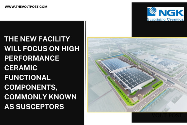
The new facility will focus on high performance ceramic functional components, commonly known as susceptors, which hold silicon wafers during high temperature processing steps like plasma etching and chemical vapor deposition.
Japanese ceramics major NGK Insulators, best known for its advanced ceramic substrates and insulators, is making a big bet on the semiconductor sector with a new plant in Ishikawa Prefecture.
The company has announced an investment of about ¥70 billion, roughly INR 4,200 crore, to build the NGK Ceramic Device Ishikawa Plant in Nomi City, an expansion that will lift its production capacity for critical ceramic components used in semiconductor manufacturing equipment by about 20 percent.
The new facility will focus on high performance ceramic functional components, commonly known as susceptors, which hold silicon wafers during high temperature processing steps like plasma etching and chemical vapor deposition.
These parts must withstand extreme heat, corrosive gases and rapid thermal cycling, and NGK is leaning on its deep expertise in alumina based ceramics to deliver highly stable, defect free materials that support next generation fabs running at smaller nodes.
The Ishikawa plant will sit on about 104,000 square meters of land adjacent to an existing NGK automotive components facility, giving the group access to shared infrastructure while maintaining a dedicated semiconductor ceramics footprint.
With a total floor area of roughly 51,000 square meters, the site is sized to ramp as global demand for advanced logic, memory and power semiconductors keeps climbing.
For NGK, this investment is part of a broader strategic shift toward the Digital Society pillar of its long term vision, alongside decarbonization linked businesses like ceramic substrates for catalytic converters and advanced battery materials.
The Ishikawa expansion consolidates its role as a key enabler of the semiconductor supply chain, even as it works with equipment makers and foundries that increasingly rely on specialized ceramics to maintain yield, reliability and process control.
NGK’s move highlights how much of the semiconductor race is being fought not just in silicon, but in the materials that sit around it are insulators, substrates and wafer handling components that quietly keep advanced fabs alive.
 By locking in additional capacity well ahead of fab expansions, NGK Insulators is positioning itself as a steady bottleneck buster in a market where the smallest material defect can ripple through an entire production line.
Mass production is scheduled to start in October 2029, with construction set to begin in April 2027, creating a core workforce of about 150 employees initially and growing to around 250 at full capacity.
