


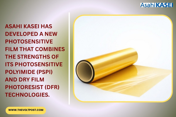
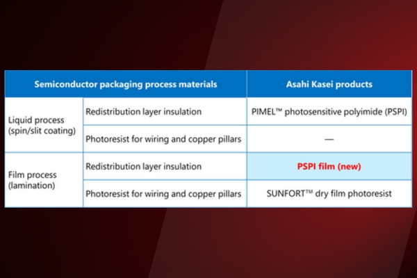
The PSPI film can be used in redistribution layers and as insulating material for package substrates.
Panel-level packaging is quickly gaining traction across the semiconductor industry, as manufacturers look for ways to boost efficiency and improve yields for next-generation packaging. Responding to this shift, The material is currently undergoing customer evaluation and is expected to be commercially available soon.
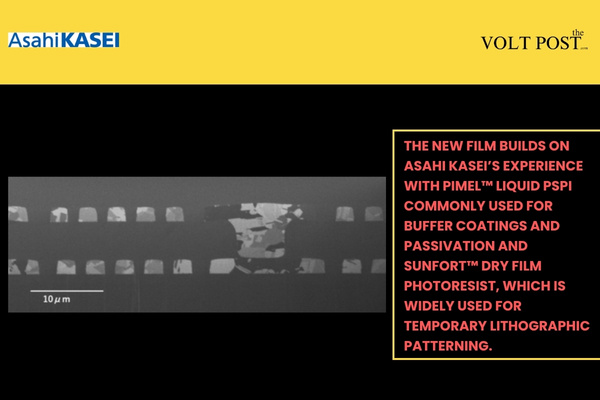
The new film builds on Asahi Kasei’s experience with PIMEL™ liquid PSPI commonly used for buffer coatings and passivation and SUNFORT™ dry film photoresist, which is widely used for temporary lithographic patterning.
By merging these capabilities into a film format, the company aims to simplify manufacturing while improving uniformity, particularly for large square panels.
The approach also supports a higher number of insulating layers, making it well-suited for advanced semiconductor packaging applications.
In practical terms, the PSPI film can be used in redistribution layers and as insulating material for package substrates. When paired with the SUNFORT™ TA series, which supports circuit patterning down to 1.0 ?m, manufacturers can form both fine wiring patterns and insulating layers through a streamlined lamination process.
 Asahi Kasei is also working on integrating the film with its SUNFORT™ CX series to enable the formation of high-aspect-ratio copper pillars, a key requirement for 3D semiconductor packaging.
Electronics remains a core focus area for Asahi Kasei under its “Trailblaze Together” strategy. Materials like PIMEL™ PSPI and SUNFORT™ photoresists are already widely used in advanced packaging, and demand is only increasing.
As chips become more densely packed and interposers grow larger particularly for AI data center applications packaging technologies are evolving rapidly. This includes a shift from wafer-level to panel-level processes, finer wiring patterns, and more complex multilayer structures, all of which are driving the need for higher-performance materials.
 Leadership Comment
Nobuko Uetake, Senior Executive Officer of Asahi Kasei with responsibility for the Electronic Materials MBU, commented, “As the performance of AI semiconductors improves, advanced semiconductor packaging requires mounting technologies that cover larger areas and offer higher precision. Through our new PSPI film product, we aim to contribute to our customers’ improved yield and productivity, while supporting the further evolution of advanced semiconductor packaging.”
To Know More: CLICK HERE
