


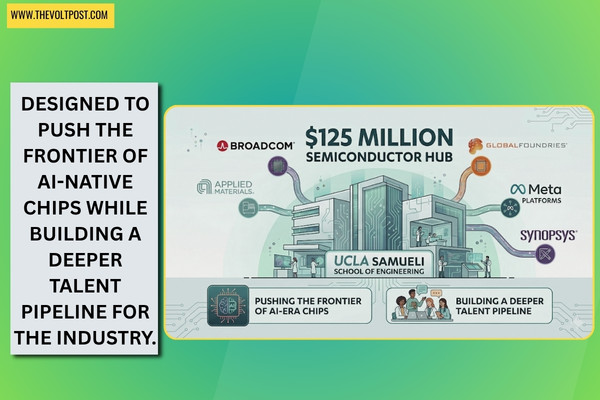
Broadcom, Applied Materials, GlobalFoundries, Meta Platforms and Synopsys are teaming up with the UCLA Samueli School of Engineering on a new $125 million Semiconductor Hub designed to push the frontier of AI-Native chips while building a deeper talent pipeline for the industry.
A $125M bet on AI-native silicon
Backed by a five-year mix of financial commitments and in-kind support, the hub will sit inside UCLA Samueli and act as a long-term collaboration platform spanning chip design, manufacturing, software, equipment, advanced materials and cloud infrastructure.
The goal is to develop “AI?native” hardware and software systems conceived from the outset around AI workloads rather than retrofitted onto legacy architectures.
Research efforts will zero in on energy-efficient architectures, advanced packaging, thermal management, ultra-broadband communications and next-generation computing platforms for edge and mission-critical use cases including robotics, autonomous vehicles, environmental monitoring and space systems.
The vision is to move beyond traditional scaling limits and enable new computing modalities that can keep up with rapidly rising AI demand without blowing out power and cooling budgets.
Linking research, fabs, EDA and the cloud
The founding partners are clearly positioning this as more than a branding exercise; they are trying to wire together a full-stack ecosystem from foundry and packaging to EDA tools and hyperscale infrastructure.
Broadcom Semiconductor Solutions Group president Charlie Kawwas said the hub will knit together foundries, silicon, packaging, equipment, electronic design automation and cloud platforms while helping train the next wave of engineering talent.
Applied Materials CEO Gary Dickerson framed it as the kind of tight industry–academia collaboration that becomes essential as device complexity and AI roadmaps accelerate, arguing it can help move breakthrough process and materials research into production faster.
GlobalFoundries CEO Tim Breen highlighted that the hub is structured to attack cross-industry technology pain points rather than just point problems while reinforcing U.S. innovation capacity and workforce depth in strategic semiconductor domains.
Synopsys CEO Sassine Ghazi stressed that future AI systems will only scale if the industry co-designs across software, hardware, electronics and physics “from silicon to system,” and said Synopsys will lean in with its AI-driven design platforms to help realize compute-efficient intelligence at scale.
Meta’s AI infrastructure lens
From the hyperscaler side, Meta engineering leader Yee Jiun Song framed the partnership squarely in terms of AI infrastructure bottlenecks. She said the hub will tackle some of the most pressing computing challenges from energy-efficient chip design to advanced packaging so that AI infrastructure can keep scaling without running into hard limits on power, bandwidth and thermals.
The timing lines up with a broader industry surge in AI capex, as major cloud and platform companies continue to pour money into data center builds and accelerator fleets to keep up with model training and inference demand, a trend regularly flagged on CNBC and other financial outlets.
By anchoring this hub inside a leading engineering school, the partners are effectively trying to point some of that infrastructure momentum back into pre-competitive research and workforce development.
Talent, internships and high-risk research
The Semiconductor Hub will fund doctoral-level research at UCLA Samueli and offer yearlong internships for engineering Ph.D. students across the founding companies, giving students a rare combination of deep academic mentorship and extended exposure to real-world design, manufacturing and deployment challenges.
Dean Ah-Hyung “Alissa” Park told CNBC that this model is meant to help students build more durable engineering and research careers by tightly coupling fundamental work with industry priorities.
Park also emphasized that the hub is explicitly structured to support high-risk, high-reward projects problems that may take years to mature but could meaningfully shorten the path from lab prototype to commercial technology if they succeed.
UCLA Chancellor Julio Frenk framed the initiative as a way for UCLA to help scale semiconductor innovation in domains critical to U.S. economic competitiveness and national security, while convening leaders across technology and policy around the next wave of intelligent systems.
