



Polymatech Electronics has commissioned a sapphire ingot crystal-growth puller at its Oragadam campus in the SIPCOT Hi-Tech SEZ near Chennai, marking a major step in its move upstream into semiconductor materials and deeper vertical integration across the value chain.
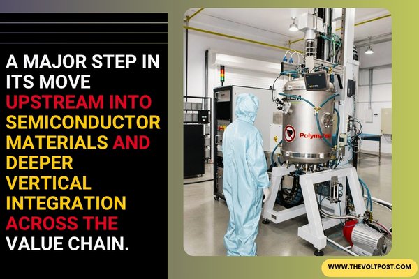
The new tool extends Polymatech’s scope from crystal growth and wafer preparation through to semiconductor packaging and finished devices, tightening control over critical materials and processes as the company scales.
Methodical ramp-up at Oragadam
The puller is currently in a rigorous process-qualification and operational-validation phase. During this stage, Polymatech is testing the stability of key utilities and operating conditions from power quality and ultra-pure water to process gases, thermal profiles and other parameters to meet the stringent requirements of reproducible single-crystal sapphire growth.
True to the company’s disciplined engineering culture, the process is being brought up deliberately rather than rushed, with each step validated before moving to the next.
The furnace is designed to grow a 100 mm diameter sapphire ingot over five working days, yielding an approximate usable length of 330 mm after cutting and grinding.
From ingot to epi-ready wafers
Once qualified, each ingot passes through precision slicing, grinding, lapping and polishing to reach an epi-ready surface finish suitable for device fabrication. At steady state, a single puller is expected to produce around 18,000 epi-ready sapphire wafers per year.
For micro-scale device geometries, that wafer output can translate into several billion semiconductor dies annually, underscoring the strategic impact of the new capacity.
Beyond near-term output, the Oragadam installation serves as Polymatech’s reference platform for crystal growth, it is the environment in which process recipes, operating discipline and qualification methodologies are developed before being replicated and scaled across multiple tools.
Foundation for Nava Raipur scale-up
The successful commissioning in Chennai sets the process baseline for Polymatech’s next phase of expansion.
Additional sapphire ingot pullers will be installed at the notified Polymatech SEZ in Nava Raipur, Atal Nagar, Chhattisgarh, as the Group builds out advanced semiconductor materials manufacturing in India.
The SEZ at Mandir Hasaud, spanning 10.13 hectares, has been formally notified by the Government of India’s Ministry of Commerce and Industry for semiconductor and electronic component manufacturing. It is expected to become a key platform for Polymatech’s next wave of growth in semiconductor materials, components and advanced manufacturing.
Cross-border sapphire capability
Polymatech’s Indian sapphire expansion is designed to complement its existing sapphire ingot and wafer operations in Grenoble, France. Together, these sites strengthen a cross-border materials capability that pairs European expertise in sapphire with Indian process engineering and manufacturing scale.
This approach mirrors the Group’s broader manufacturing footprint across India, Singapore, France, Estonia and the United States.
In each geography, Polymatech has pursued a strategy of pushing deeper into critical materials and process technologies rather than relying solely on downstream assembly.
A deliberate model of vertical control
The sapphire programme reflects Polymatech’s operating model: develop technology and process capability through disciplined engineering, validate under real production conditions, then scale proven processes through dedicated manufacturing assets across the Group.
In that context, the Oragadam installation is more than a single tool. It is a crystal-growth hub, a process-qualification reference and the template for future multi-puller deployments. By tightening control over materials, process engineering, packaging and finished-device production, Polymatech is betting that resilient semiconductor manufacturing depends on vertical capability, not just on assembly capacity.
 Leadership Comment
“In our industry, light begins in the crystal. We have grown this capability the way we have grown everything — patiently, precisely, and through disciplined engineering. The commissioning at Oragadam gives us the process platform; the notified Polymatech SEZ at Nava Raipur gives us the opportunity to carry that capability to industrial scale.
Our objective is clear: to build deeper control over the semiconductor value chain, from the first crystal to the finished chip, while creating globally competitive manufacturing capability from India.”
— Eswara Rao Nandam, Managing Director & CEO, Polymatech Electronics Limited
Consistent with this philosophy, the programme, like every facility in Polymatech’s five-country footprint has been conceived, engineered and funded entirely from the Group’s own resources, underscoring a long-term commitment to building semiconductor infrastructure on its own balance sheet.