


Intel Foundry Services has unveiled a major breakthrough with what it says is the world’s thinnest gallium nitride (GaN) chiplet. The silicon substrate has been thinned to just 19 micrometers, or about one-fifth the width of a human hair.

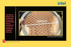
The chiplet is built on a 300 mm GaN-on-silicon wafer using Intel’s proprietary stealth dicing and thinning process, which helps achieve an ultra-thin form factor without sacrificing structural strength or performance stability.
What makes this development especially notable is that Intel has, for the first time, integrated GaN power transistors with silicon-based digital logic circuits on the same chiplet.
That means more computing functions can be built directly into the power device itself, reducing the need for extra auxiliary chips and simplifying the overall system design.
Performance results are also impressive. The GaN transistors can handle voltages up to 78 V and reach a radio-frequency cutoff of more than 300 GHz, making them well suited for high-frequency communication applications.
Intel’s integrated digital logic library also performed reliably, with inverter switching speeds as fast as 33 picoseconds and consistent results across the wafer, both of which point to strong mass-production potential.
The technology has passed four industry-standard reliability tests as well, showing it can withstand high-temperature and high-voltage conditions and meet commercial deployment requirements.
 This matters because traditional silicon is getting close to its limits in high-power and high-frequency applications. GaN, as a wide-bandgap semiconductor, offers higher power density, faster switching, and lower energy loss.
By using 300 mm GaN-on-silicon wafer processing, Intel Foundry Services’ approach should also fit into existing semiconductor manufacturing lines, which could help lower production costs and speed up adoption.
To Know More: CLICK HERE
