


Washington State University (WSU) researchers have unveiled a groundbreaking layered semiconductor structure with enormous potential to transform next-generation data storage.
By leveraging two-dimensional (2D) materials, this discovery could pave the way for more energy-efficient, compact, and flexible electronics used in everything from smartphones and wearables to artificial intelligence (AI) systems and cloud data centers.
The study, published in the Small Science journal, signals a pivotal moment in semiconductor engineering. With traditional silicon-based technologies approaching physical limits, this new architecture—called a “van der Waals heterostructure”—offers a scalable, low-power alternative.
What Are Layered Semiconductors?
The Role of 2D Materials in Modern Electronics
Layered semiconductors utilize ultra-thin materials just a few atoms thick, stacked in precise configurations. One of the key materials used in this research is molybdenum disulfide (MoS?), a 2D material known for its unique electronic and optical properties.
These van der Waals heterostructures are held together not by chemical bonds, but by weak van der Waals forces. This allows scientists to design entirely new materials with custom-built properties for data retention, energy efficiency, and miniaturization.
Key Features and Benefits
1. High-Speed Data Writing and Retention
The Washington State University team’s new semiconductor configuration allows data to be written quickly and retained over long periods. This is particularly useful for non-volatile memory, which stores data even when the power is turned off.
2. Low Power Consumption
Devices built on this technology use significantly less energy than traditional semiconductor memory systems, making them ideal for applications where power efficiency is crucial—such as edge computing, IoT sensors, and wearable electronics.
3. Flexibility and Miniaturization
The atomic thinness of these 2D materials supports flexible electronics, enabling innovations in rollable displays and bendable devices while supporting the growing demand for miniaturized tech solutions.
Expert Commentary on the Breakthrough
Saptarshi Das, Penn State University
“This material will let us capture the best of both worlds: storage and computation,” said Das, who is working on hybrid semiconductors that integrate memory and logic capabilities. “It opens new doors for computing architectures that are both faster and more efficient.”
Dr. Huamin Li, University at Buffalo
“Our research explores how these layered materials can be married with traditional silicon. The aim is to boost performance while keeping manufacturing costs in check,” said Dr. Li. “This paves the way for energy-efficient nanoelectronics.”
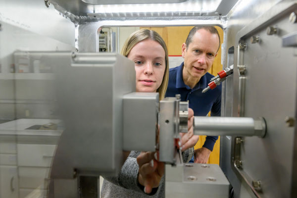
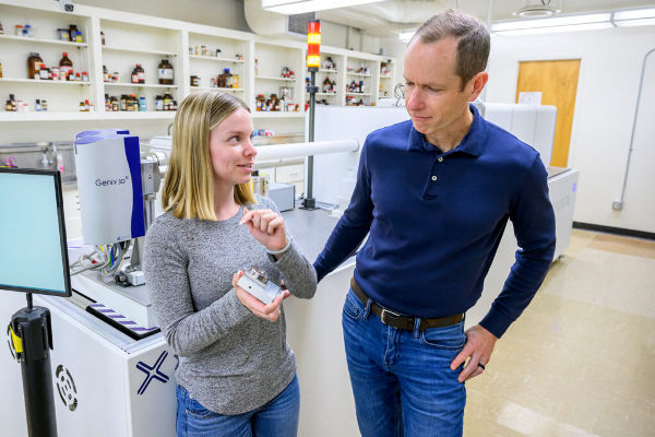
Dr. Weijie Huang, Lead Author (Washington State University School of Electrical Engineering and Computer Science)
“This is one of the first demonstrations of a van der Waals heterostructure made of two types of 2D semiconductors with a large valence band offset,” Dr. Huang said. “This offset is critical for storing and releasing electrical charges.”
Real-World Applications and Industry Impact
A New Era for Non-Volatile Memory
Non-volatile memory—used in USB drives, SSDs, and mobile devices—requires materials that can retain data without continuous power. The WSU device’s charge trapping layer enables this function with greater stability and fewer leaks.
Enabling AI and Edge Computing
In artificial intelligence and edge computing environments, speed, compact size, and efficiency are key. Layered semiconductors offer all three, helping neural networks and smart sensors process data closer to the source, reducing latency and power usage.
Role in Flexible and Wearable Tech
As the world moves toward smart fabrics, wearable health monitors, and bendable smartphones, 2D materials like MoS? become indispensable. Their flexible nature allows engineers to design devices that are not only high-performing but also comfortable and durable.
Market Forecast: What’s Next?
Rising Demand for Layered Semiconductor Solutions
The global market for 2D material-based semiconductors is expected to grow rapidly over the next five years. According to a 2024 report by Semiconductor Insight, demand is being driven by:
- The rollout of 6G and AI-powered IoT networks
- The need for low-energy memory in mobile computing
- Increased adoption of flexible displays and wearable devices
Barriers and Challenges
Despite the promise, integrating 2D materials with existing silicon-based fabrication remains a technical challenge. Large-scale manufacturing of van der Waals heterostructures still requires precision and cost-effective processes.
Ongoing research is focused on improving transfer techniques, layer uniformity, and compatibility with CMOS technology to make these solutions viable for mass production.
Academic Collaboration and Research Support
The study was led by researchers at Washington State University’s School of Electrical Engineering and Computer Science and published in the Wiley journal Small Science. Funding and collaboration also came from:
- The U.S. National Science Foundation (NSF)
- The Washington Research Foundation
- The Department of Energy’s Office of Science
Transforming the Future of Electronics
The layered semiconductor developed by Washington State University marks a significant leap toward high-speed, energy-efficient, and compact memory solutions. It aligns with the broader industry shift toward post-silicon technologies that can meet the growing demands of the digital age.
