


The domestic semiconductor market in India is projected to more than triple over the next decade as local demand for advanced digital infrastructure accelerates. A comprehensive new report named Semicon India 2.0 authored by EY and IESA estimates the sector will expand from its current $64 billion valuation in 2026 to an impressive $200 billion by 2035.
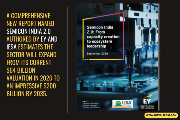
Titled Semicon India 2.0 the analysis frames this rapid expansion as a critical window for the domestic semiconductor market in India to shift from relying on imported silicon to building a highly resilient domestic manufacturing ecosystem.
Emerging Tech Fuels Demand
Consumer electronics currently anchor the market by driving 30 percent of total semiconductor consumption in the country.
Automotive and industrial applications follow closely representing 16 percent and 15 percent respectively. Yet the most significant future growth is expected to stem from next generation digital infrastructure.
The unprecedented surge in artificial intelligence compute requirements, hyperscale data centers, telecommunications expansion and electric mobility are creating massive new avenues for advanced chip consumption.
The Push for Local Fabrication
This soaring demand is currently being met primarily by international suppliers. The report highlights that semiconductor imports grew fivefold over recent years jumping from $5.7 billion in fiscal year 2017 to over $30.3 billion in fiscal year 2025. That trajectory represents a staggering 23 percent compound annual growth rate.
For industry stakeholders this rising import reliance underscores the urgent need to establish local wafer fabrication and advanced packaging facilities.
Government officials and industry leaders agree that the national semiconductor narrative has successfully moved past ambition and initial policy announcements and is now focused squarely on commercial production and ecosystem building.
Capitalizing on Engineering Talent
India holds a unique structural advantage as the nation already houses nearly 20 percent of the global chip design engineering workforce.
The EY and IESA roadmap in Semicon India 2.0 suggests leveraging this robust existing talent base to scale up actual hardware manufacturing and commercialization.
To convert current momentum into long term global competitiveness the report recommends developing integrated manufacturing clusters backed by world class shared infrastructure.
Additionally experts stress the importance of rolling out targeted talent certification programs, streamlining regulatory approvals and aligning state level policies to ensure stable growth for the rapidly expanding domestic chip sector.
Leadership Comments
 Ashok Chandak, President, India Electronics and Semiconductor Association (IESA) said, “India now has a unique opportunity to combine its strengths in engineering talent, electronics demand, design capabilities and emerging manufacturing capacity with resilient global supply-chain partnerships. The next phase will be defined by execution, innovation, technology commercialisation, indigenous IP, specialised talent and ecosystem depth. India has moved beyond semiconductor ambition. The opportunity now is to build an ecosystem that the world trusts, India owns and the next generation can scale.”
Aisha Ali Hussaini, Partner and Semiconductor Tax Leader, EY India, said, “India has a powerful combination of market scale, engineering talent and policy momentum. Its rapidly expanding electronics ecosystem adds to this opportunity; electronics production increased sixfold from INR1.9 lakh crore in FY15 to INR11.3 lakh crore in FY25, while electronics manufacturing and exports grew sevenfold and elevenfold, respectively, over the same period. The priority now is to translate this scale into deeper semiconductor value addition by building a connected, innovation-led ecosystem that attracts sustained investment and creates more value domestically.”
“Over the coming decade, a predictable fiscal and regulatory environment, stronger alignment between central and state policies, and focused support for emerging technologies can help improve project viability and accelerate commercialisation. If industry, government and academia work together with a long-term view, India can move beyond being a design powerhouse to play a much larger role across manufacturing, advanced packaging and the wider global semiconductor value chain,” concluded Hussaini.
To Download The Full Report: CLICK HERE