


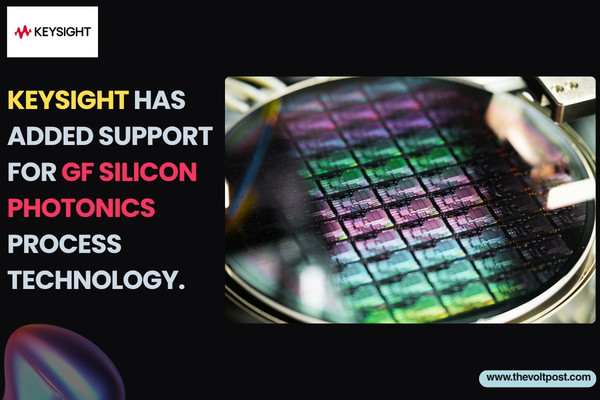
Keysight Technologies has added support for GlobalFoundries’ (GF) silicon photonics process technology in its Advanced Design System (ADS) Photonic Designer, expanding its ecosystem for photonic integrated circuit (PIC) development.
The integration allows engineers to move seamlessly from PIC design to full electro-optical-electrical (EOE) system simulation within a single environment making it possible to validate optical link performance before tapeout.
As silicon photonics scales into volume deployment across data centers, AI infrastructure, and high-speed optical networks, designing a PIC is only one part of the equation.
The bigger challenge lies in understanding how that design performs within a complete EOE system. Traditionally, this requires switching between separate design and simulation tools, often delaying validation and introducing risk late in the development cycle.
Keysight’s new PDK for ADS Photonic Designer addresses this gap by bringing PIC design and system-level simulation together. Engineers can design photonic circuits on GF’s platform and immediately evaluate full optical link behavior including eye diagram analysis and key signal integrity metrics such as transmission dispersion eye closure quaternary (TDECQ) without leaving the environment.
The PDK is built on physics-based models aligned with GF’s silicon photonics process, ensuring simulation results closely match fabricated silicon. At the same time, system-level validation provides early confidence that the overall channel link performance will meet requirements.
This level of integration is particularly valuable for high-speed optical interconnect development, especially in applications like optical transceivers and co-packaged optics, where photonic and electronic performance must be verified together. Engineers can also leverage Keysight’s FlexDCA oscilloscope software during the design phase, improving correlation between simulation and real-world measurements and enabling more accurate predictive modeling.
Key advantages include:
- Faster design start: Ready-to-use, foundry-aligned models eliminate the need to build and calibrate component libraries from scratch.
- Pre-tapeout confidence: FlexDCA-based measurement simulation and TDECQ analysis help reduce design-to-test discrepancies and improve predictability.
- Earlier system insight: By shifting validation earlier in the workflow, teams can assess how PIC performance impacts the full optical link, reducing iterations and accelerating time to market.
The GlobalFoundries CLO PDK for ADS Photonic Designer is now available.
 Leadership Comments
Vikas Gupta, Senior Fellow, Silicon Photonics Product Line at GlobalFoundries, said: “As silicon photonics moves into broader deployment for AI infrastructure and high-speed optical communications, designers need workflows that connect device innovation with system-level performance from the start. By enabling our silicon photonics platform in Keysight’s ADS Photonic Designer, we’re helping customers accelerate development, reduce design risk and scale their optical interconnect solutions more effectively.”
Niels Faché, Senior Vice President, Keysight’s Design Engineering Software, said: “The silicon photonics industry has moved past the point where circuit design and system validation can live in separate workflows. Engineers building for AI and data center infrastructure need to see system-level link performance from day one, not after fabrication.”
To Know More: CLICK HERE
