


India’s electronics and semiconductor design talent pool is one of the world’s largest and most skilled. From Bengaluru’s sprawling design hubs to Noida’s emerging tech corridors, engineers across the country are powering everything from automotive chips to AI accelerators. But behind the headlines of India’s $103 billion semiconductor market projection by 2030 and booming ESDM ecosystem, Design Engineers in India are grappling with real, day-to-day hurdles that threaten to slow this momentum.
If you’re a design engineer in India or leading a team you know the pressure is intense. Deadlines are tight, expectations are sky-high, and the gap between global standards and local realities feels wider than ever.
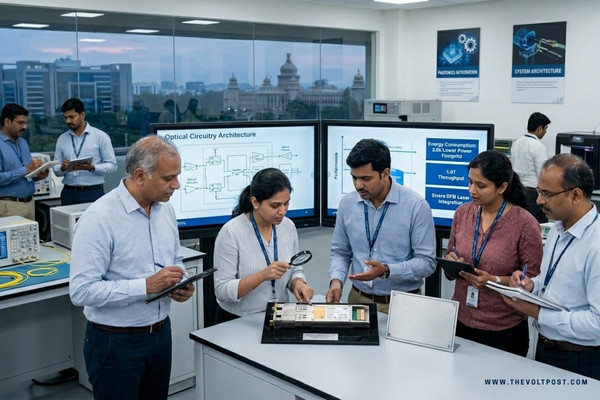
Let’s fractionate the top challenges facing design engineers in India today, straight from the factory floors, design labs, and industry forums. These aren’t abstract problems; they’re the bottlenecks showing up in your VLSI flows, PCB layouts, and system verifications right now.
Chronic Talent and Skill Gaps in Cutting-Edge Domains
India produces 1.5 million engineering graduates annually, yet the semiconductor industry faces a 200,000-talent shortage projected by 2027. Design engineers tell us the real pain point isn’t sheer numbers it’s specialized skills in areas like 3nm/2nm process nodes, high-frequency RF design, and advanced packaging.
Take VLSI design, for instance. While Tier-1 colleges like IITs and NITs churn out solid analog and digital designers, the industry needs more experts in RISC-V architecture, chiplet-based SoCs, and AI/ML hardware optimization. “We’re hiring fresh grads who know SPICE simulations but struggle with real-world DFT (Design for Testability) flows,” shares a senior design lead at a Hyderabad fabless startup.
 The mismatch hits harder in Tier-2/3 cities where design centers are expanding but training infrastructure lags. Engineers there often juggle legacy 28nm projects while upskilling for 5nm tape-outs on personal time through YouTube tutorials or late-night Online courses.
Aggressive industry-academia partnerships like ISM 2.0’s skill initiatives are helping, but engineers need hands-on access to PDKs (Process Design Kits) and EDA tools like Cadence Innovus or Synopsys Fusion Compiler. Without it, India’s design ambition stays stuck in the “good enough” zone.
EDA Tool Access and Cost Barriers
Imagine architecting a complex SoC but hitting license timeouts on your Cadence Virtuoso suite every two hours. This is daily life for many design engineers in India, where EDA tool costs can eat 30-40% of a small design house’s budget.
Global giants like Synopsys, Cadence, and Siemens EDA charge premium prices, and while multi-year licenses help large players like Qualcomm India or Intel Bangalore, startups and mid-sized firms in Gurgaon or Chennai struggle. “Cloud-based EDA is the future, but latency from Indian data centers kills productivity during DRC runs,” admits an RF design engineer from a Delhi-NCR firm.
 Open-source alternatives like OpenROAD or SkyWater PDK show promise, but they’re not production-ready for commercial 7nm designs. Engineers end up pirating tools (a risky move) or sharing licenses across teams, compromising security and IP protection.
India’s 100% FDI in electronics manufacturing draws design work home, but without subsidized EDA access, engineers waste hours on workarounds instead of innovation. Government schemes like the Design Linked Incentive (DLI) under PLI 2.0 are a start, but they need to cover tool subscriptions directly.
Infrastructure Woes – Power, Nets, and Compute
Design engineers in India don’t just battle code they fight frequent power cuts, erratic internet, and underpowered workstations.
In Bengaluru’s Electronic City, rolling blackouts disrupt timing closure runs that need 24/7 compute. “A single outage can set back a multi-week STA (Static Timing Analysis) by days,” says a physical design engineer.
High-speed internet is another pain. Uploading 100GB Synopsys test vectors to a US-based fab partner?
Good luck with India’s internet Providers peak-hour throttling. And don’t get started on GPUs, NVIDIA A100s for ML model training are either unavailable or priced at enterprise levels, forcing engineers to rely on spotty cloud instances from AWS Mumbai.
Co-working design hubs in India are popping up, offering reliable power and NVLink clusters, but they’re expensive for freelancers or small teams. As India’s ESDM exports target $120 billion by 2026, reliable Tier-3 data centers with low-latency EDA farms can’t come soon enough.
Supply Chain Disruptions Hitting Prototyping
India’s design engineers excel at RTL-to-GDSII, but fab access remains a chokepoint. With no domestic sub-7nm foundry yet, tape-outs go to TSMC or GlobalFoundries, facing 6-9 month lead times amid US-China tensions.
Prototyping is worse. FPGA emulation boards with Xilinx Versal or Intel Agilex are scarce and backordered, thanks to global chip shortages lingering into 2026.
“We designed a 5G mmWave chipset in Gurugram, but validating it took three months longer because of PCB fab delays in Shenzhen,” recounts a wireless design lead.
Local options like Bengaluru’s SCL or Mohali’s semi-fab handle simple ASICs, but advanced packaging (CoWoS, InFO) is outsourced. Engineers resort to virtual prototyping in Siemens Veloce, but nothing beats silicon validation. As OSAT facilities like Kaynes and SPEL scale, India needs faster domestic MPW (Multi-Project Wafer) shuttles to close the loop.
IP Licensing Costs and Localization Mandates
Global IP cores from Arm, Synopsys, or Cadence are gold for fast time-to-market, but licensing fees sting Indian design houses. A single Arm Cortex-A78 core can cost $1M+ upfront, pricing out all but the biggest players.
Make in India policies push localization, but creating indigenous IP from scratch? That’s a 3-5 year slog with no revenue. “We’re reverse-engineering basic SerDes for automotive ECUs because premium IP is unaffordable,” reveals a Pune-based team lead.
The irony is that India’s 1.2 million design engineers could build world-class IP in power electronics or IoT sensors, but short project cycles favor off-the-shelf blocks. Initiatives like India Chipset Mission aim to fund homegrown IP, but engineers need venture capital to de-risk the R&D.
Work-Life Imbalance and Brain Drain Pressures
Long hours are the norm in India’s design world. 60-70 hour weeks during tape-out crunch times lead to burnout, especially in high-pressure hubs like Hyderabad’s HITEC City. “Tape-out Fridays mean 2 AM finishes, then straight to Saturday debug,” laughs (bitterly) a digital design engineer.
Worse, brain drain looms large. US firms like NVIDIA and Apple poach top talent with 2-3x salaries and H1B visas. A senior verification engineer in India might earn ?40-50 lakhs; the same profile in California pulls $200K+. With family pressures and inflation, many jump ship.
India’s counter is with ESOP-rich startups like Saankhya Labs or Tata Elxsi retain talent, but engineers crave mentorship and career paths beyond “lead to manager.” Flexible WFH post-COVID helps, but client calls from California at 8 PM IST don’t.
Regulatory and Compliance Headaches
Navigating MeitY approvals for controlled tech, export compliance under SCOMET, and data localization under DPDP Act adds layers of bureaucracy.
“Clearing a crypto-ASIC design for export took six weeks of paperwork,” gripes a Bengaluru security IP specialist.
ESG mandates are creeping in too. EU’s Carbon Border Adjustment Mechanism hits exported chips, forcing engineers to optimize for low-power designs amid power-hungry AI workloads. India’s green electronics standards are evolving, but inconsistent state-level incentives confuse teams.
The Road Ahead for India’s Design Engineers
India’s design engineers aren’t just surviving these challenges they’re innovating around them.
From open-source RISC-V hubs in Coimbatore to 5G testbeds in Chennai, resilience defines the community.
But to hit $400 billion in electronics manufacturing by 2030, India needs:
- Subsidized EDA and fab shuttles via PLI extensions
- Upskilling bootcamps tied to industry PDKs
- Tier-3 data centers optimized for compute-intensive flows
- IP funds for indigenous cores in EV, renewables, and defense
References:
- $103B semiconductor market by 2030: India Manufacturing Review, IESA Report
- 200K talent shortage: Deloitte 2026 Outlook
- EDA costs (30-40%): Semiconductor EDA Market Report
- Brain drain (?40-50L vs $200K): Levels.fyi India Data, CIO Salary Report
- SCOMET/Regulatory delays: India Briefing SCOMET Guide
- ISM 2.0 & PLI/DLI: PIB Press Release
