



Infineon Technologies is making a massive leap in power electronics by setting up the world’s first high-volume manufacturing plant for 300mm wafer GaN power semiconductors. Located at the company’s innovation hub in Villach, Austria, the landmark facility positions Infineon to capture a dominant share of the rapidly expanding wide-bandgap chip sector.
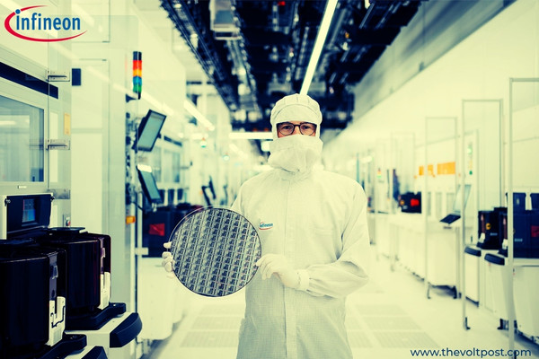
The transition to 300mm wafer GaN power semiconductors, or 12 inch, silicon-based GaN production represents a critical structural upgrade for the semiconductor sector.
Larger wafer sizes deliver roughly 2.3 times more chips per wafer compared to standard 200mm lines, dramatically improving yield efficiency and lowering cost structures for next-generation power architectures.
Scaling for High Performance Infrastructure
Gallium nitride technology operates at significantly higher efficiency levels and switching speeds than traditional silicon.
These physical advantages mean power converters can shrink in physical size while handling greater power densities with minimal thermal loss.
The timing aligns directly with severe power demand challenges hitting global energy infrastructure. Heavy computational workloads in artificial intelligence data centers, combined with rapid expansions in e-mobility, solar energy conversion, and robotics, require unprecedented energy efficiency from grid to chip.
Key advantages driving wide-scale GaN adoption include:
- Massive Efficiency Gain: Drastically reduces power loss in high-voltage server racks and power supply units.
- Compact Footprint: Allows hardware designers to shrink transformers, capacitors, and overall power module dimensions.
- Enhanced Production Economics: Scaling onto 300mm lines brings economies of scale previously reserved for conventional silicon chips.
Building a Resilient European Chip Supply Chain
By upgrading existing cleanroom infrastructure at Villach rather than building a greenfield site, Infineon is expanding its total output with maximum capital efficiency.
The 300mm wafer GaN power semiconductors line project benefits from key European chip initiative funding designed to strengthen local semiconductor manufacturing resilience and  technology leadership.
The site also merges commercial volume manufacturing directly with local research and development teams, speeding up the cycle from initial chip design to full market deployment.
As global industries race to decarbonize compute infrastructure and industrial automation, high-volume 300mm GaN production ensures energy-efficient chips will be available at scale to power the next generation of tech hardware.