


India took a meaningful step toward advanced electronics self-reliance on recently with the launch of indigenously developed silicon photonics solutions at IIT Madras in Chennai.
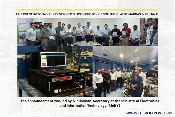
The announcement was led by S. Krishnan, Secretary at the Ministry of Electronics and Information Technology (MeitY), and introduced two important developments, a Silicon Photonics Process Design Kit (PDK) and a Universal Programmable Photonic Integrated Circuit (PPIC) Test Engine.
Both were developed at the MeitY-supported Centre of Excellence for Compound Photonics and Photonic Integrated Circuits Systems (CoE-CPPICS) at IIT Madras.
MeitY called the launch a major milestone in India’s push toward technology sovereignty in silicon photonics, an emerging field that combines optical and electronic functions on a single chip.
The platform is designed to serve as a shared national resource, supporting research and development across academia, industry, startups, and defence.
The newly launched PDK includes more than 50 verified components, giving developers a solid foundation for designing advanced photonic integrated circuits. The PPIC Test Engine, meanwhile, provides an automated environment for testing and characterising photonic and optoelectronic modules across different use cases.
Speaking at the event, Krishnan said India’s silicon photonics capabilities are now closing in on global benchmarks, but added that the next big step is building fabrication infrastructure under the India Semiconductor Mission.
Amitesh Sinha, Additional Secretary at MeitY and CEO of the India Semiconductor Mission, said the technology has relevance in both classical and emerging quantum applications. He also noted that future progress could be supported through the proposed ISM 2.0 framework, especially under its R&D focus.
The next phase of the project will enable multi-project wafer (MPW) fabrication runs from the third quarter of the current financial year. That will bring fabrication, testing, packaging, and module characterisation into a more integrated workflow.
 Built under a Product Research, Development and Manufacturing (PRDM) model, the initiative uses CMOS-compatible silicon photonics technology and is backed by both global and domestic partners, including SilTerra Malaysia as the foundry partner and izmo Microsystems, Bengaluru, for photonic IC packaging.
