


IBM has unveiled a major semiconductor breakthrough with what it calls the world’s first sub-1 nanometer chip technology, built on a new 0.7 nm (7 angstrom) node. The development comes at a time when the industry is grappling with the physical limits of traditional scaling, marking an important step forward for next-generation computing.

The new chip packs nearly 100 billion transistors into a footprint roughly the size of a fingernail almost double the density of IBM’s 2 nm chip introduced in 2021.
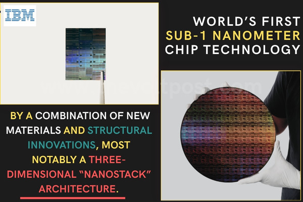
This leap is made possible by a combination of new materials and structural innovations, most notably a three-dimensional “nanostack” architecture that pushes performance and efficiency gains even as features approach atomic-scale dimensions.
According to IBM, the technology could deliver up to 50 percent higher performance or 70 percent better energy efficiency compared to its 2 nm node.
That kind of improvement could significantly boost workloads across generative AI, cloud infrastructure, and future electronic devices.
Nanostack: A New Architecture
At the core of this breakthrough is nanostack, a completely new transistor design that builds on and goes beyond today’s nanosheet technology. Instead of laying transistors out in a single plane, nanostack stacks and staggers them vertically using 3D sequential integration.
This approach allows more transistors to fit into the same area while also enabling different materials to be used in each layer, optimizing performance and power at a much finer level.
IBM researchers have already demonstrated that the concept works in practice. They validated the architecture using ultra-thin dielectric bonding in CMOS integration, showed dual-channel engineering capability, and successfully operated functional CMOS inverters with expected switching behavior. Together, these results confirm that nanostack is not just theoretical—it can support real computation.
In related work presented at VLSI 2026, IBM also showed that nanostack enables around 40 percent scaling in SRAM, opening the door to more efficient chips that can better handle the high-bandwidth demands of advanced AI workloads.
This architecture effectively extends logic scaling below the 1 nm threshold for the first time, ushering in the angstrom era, where chip features approach the size of individual atoms. While node names today reflect technology generations rather than exact physical dimensions, IBM’s 0.7 nm milestone demonstrates that meaningful scaling progress is still achievable. The company believes this approach could support at least another decade of advancement.
Built on Long-Term R&D
The announcement builds on IBM’s long history of semiconductor innovation, from early chip development in the 1960s to more recent milestones like the 2 nm node. The company continues to focus on advancing silicon technologies alongside AI hardware, logic design, and quantum computing.
Much of this work is carried out at IBM’s research facility in Albany, New York, where the ecosystem is preparing for the introduction of High NA EUV lithography.
Developed by ASML, this next-generation lithography technology will enable more precise patterning, supporting the fabrication of smaller and more powerful chips.
IBM is collaborating with partners such as Lam Research, Tokyo Electron, and SCREEN Semiconductor Solutions to develop the processes and tools needed for this transition, with early devices already demonstrated.
IBM is also expanding its ambitions beyond classical semiconductors. The company recently announced plans to establish Anderon, a standalone entity positioned as the world’s first pure-play quantum foundry. Leveraging IBM’s expertise in both quantum computing and semiconductor manufacturing, the initiative aims to strengthen domestic capabilities in quantum wafer production.
Looking ahead, the company expects that nanostack-based chips could reach production within the next five years, setting the stage for the next phase of semiconductor scaling.
Leadership Comment
“IBM’s latest chip breakthrough marks a landmark moment in computing, pushing technology beyond the nanometer era to the scale of atoms. With our new nanostack architecture, we’re not just making smaller transistors, we’re reinventing how chips are built to deliver dramatically more power and energy efficiency,” said Jay Gambetta, Director of IBM Research and IBM Fellow. “This industry-first innovation continues IBM’s legacy of leading in next-generation technologies and sets the foundation for the next era of computing.
To Know More: CLICK HERE
