


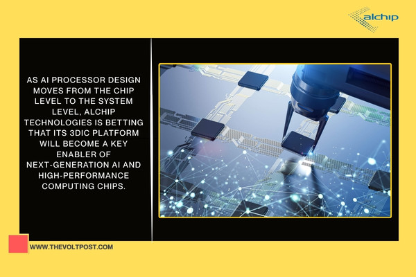
As AI processor design moves from the chip level to the system level, Alchip Technologies is betting that its 3DIC platform will become a key enabler of next-generation AI and high-performance computing chips. The idea is simple, instead of squeezing everything onto one giant die, the platform uses flexible chiplet architectures and advanced packaging to build more efficient, scalable systems.
AI infrastructure has entered a new era of system-level complexity. Raw transistor density is no longer enough. Performance now hinges on how well multiple compute dies, memory stacks, and interconnect fabrics work together as a single, cohesive system. Design teams must balance performance, bandwidth, power, thermal constraints, and manufacturability—all at the same time.
Next-gen AI accelerators need multi-terabyte-per-second memory bandwidth, and data movement is eating up an ever-larger share of total system power. Large monolithic dies are hitting reticle limits, suffering from lower yields, and pushing mask costs higher. Even conventional 2.5D approaches come with their own headaches like, interposer complexity, package size limits, and limited flexibility for stacking and vertical integration.
Alchip’s 3.5D ASIC platform tackles these issues with a system?centric approach to heterogeneous integration. It breaks large SoCs into smaller, optimized chiplets spread across different process nodes.
Compute dies scale on leading-edge technologies where performance matters most, while I/O and memory blocks stay on more cost-efficient nodes to improve yield, cut costs, and speed time-to-market.
The platform mixes horizontal chiplet scaling with selective vertical die stacking, creating a hybrid 3.5D architecture that delivers higher interconnect density and more design freedom than traditional 2.5D or monolithic approaches.
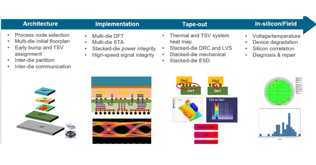
It pairs this architecture with advanced packaging technologies such as CoWoS-S, CoWoS-R, CoWoS-L, and TSMC-SoIC-X, enabling high-bandwidth, low-latency links between dies. The result is multi-terabyte-per-second aggregate throughput, with up to 3-5× higher interconnect density and 30-40% lower energy per bit at latencies cut by as much as 35% in some cases.
Beyond raw bandwidth, the platform also co-optimizes die placement, heat dissipation, and power delivery. Shorter vertical power paths and improved power-delivery networks help boost performance while easing thermal load.
Integrated thermal strategies are tuned to work with advanced data-center cooling techniques, making it easier to manage the kilowatt-class systems that AI accelerators are now targeting.
From a design-flow perspective, the 3DIC platform unifies the path from silicon to packaging to system-level implementation. It reduces the friction between these domains, allowing designers to focus on optimizing their workloads instead of wrestling with integration and packaging details.
Alchip’s 3DIC platform is targeted at hyperscale cloud providers, AI accelerator startups, and HPC system companies building custom silicon. A typical configuration might include multiple compute chiplets on advanced nodes, I/O dies on mature nodes, and high-bandwidth memory (HBM) stacks all integrated into a single package supporting systems that now operate at multi-kilowatt power levels.
By combining its long-standing strengths in advanced-node ASIC design with cutting-edge 2.5D and 3DIC integration, Alchip is positioning its 3DIC platform as a foundational building block for the next wave of system-level AI and HPC chips.
Leadership Comment
“AI innovation no longer happens at the chip level alone,” says Johnny Shen, Chairman, CEO, and President of Alchip Technologies. “It’s moving fast to the system level. Our 3DIC platform gives customers the flexibility to architect around their workloads, while we handle the complexity of integration, packaging, and volume production.”
To Know More: CLICK HERE
