


Kioxia Holdings is finally making its wafer-bonding move. The Japanese semiconductor manufacturer is launching a direct challenge to Samsung Electronics’ grip on the memory chip market, deploying advanced wafer-bonding technology for its next-generation NAND flash memory products.

Data Centers Are the Real Battleground
Demand for memory in data centers is spreading beyond traditional DRAM to include NAND flash memory.
Kioxia is known to see an opportunity and is weaponizing innovative technology to reclaim market share bringing it to market before competitors can catch up.
The company has parked a significant chunk of its investment in NAND flash memory technology, staking its position to ride the AI-driven storage boom.
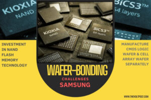
Wafer Bonding – The Kioxia’s Edge
Kioxia’s edge comes down to CMOS directly Bonded to Array (CBA) technology aka hybrid bonding. The process is straightforward, to manufacture the CMOS logic wafer and cell array wafer separately under their optimal conditions, then bond them face-to-face.
Traversing Three Vital Areas:
Kioxia’s 8th generation BiCS FLASH™ 3D flash memory puts this high-precision wafer bonding to work, hitting 218 layers with 2Tb device capacity.
Samsung’s Lead Under Pressure
Samsung still sits atop the memory chip world, but Kioxia’s advanced NAND products are designed to shake up its stagnant market share.
Memory manufacturers globally are racing to develop High-Bandwidth Flash Memory (HBF), a new technology similar to HBM (High-Bandwidth Memory) but built on NAND flash for higher capacity and better cost-effectiveness.
Partnering With Western Digital
Kioxia’s wafer-bonding technology development has been powered by an engineering partnership with Western Digital. Both companies follow a shared R&D roadmap and have pushed this fundamental technology into production ahead of schedule.
Masaki Momodomi, CTO at Kioxia Corporation:
“Through our unique engineering partnership, we have successfully launched the eighth-generation BiCS FLASH™ with the industry’s highest bit density.”
Alper Ilkbahar, Senior VP of Technology & Strategy at Western Digital:
“By working with one common R&D roadmap and continued investment in R&D, we have been able to productize this fundamental technology ahead of schedule and deliver high-performance, capital-efficient solutions.”
Kioxia’s latest 218-layer 3D flash memory brings serious specs to the table:
- 1Tb triple-level-cell (TLC) and quad-level-cell (QLC) with four planes
- 50%+ boost in bit density through innovative lateral shrink technology
- 3.2Gb/s NAND I/O speed—that’s a 60% jump from the previous generation
- 20% gains in write performance and read latency
- 8TB flash memory capacity by stacking 32 memory dies in a package under 2mm tall
Kioxia reported an $8.2 billion profit in Q1 2026, underscoring its strong footing as it pushes wafer-bonding technology forward.
Targeting data-heavy applications across the board:
- AI servers and data centers
- Smartphones
- IoT devices
- Advanced SSDs
 Kioxia has already started sample shipments to limited customers for its 8th generation BiCS FLASH™ technology. The company keeps pushing cutting-edge memory solutions as AI adoption drives exponential data growth.
With wafer-bonding technology now in mass production and Samsung developing its own HBF products, the memory chip race has entered a new phase. The fight is now about who masters hybrid bonding first.
