


OKI Circuit Technology, the OKI Group’s printed circuit board (PCB) business unit, has developed new design and production technologies for 180-layer PCB which is 15 mm-thick aimed at wafer testing equipment for high-bandwidth memory (HBM) used on AI semiconductors.
This is roughly a 45% increase in layer count and nearly double the thickness compared with the earlier 124-layer, 7.6 mm-thick configuration.
OTC is now working to finalize mass-production technology and install the necessary equipment at its Joetsu Plant, targeting start-of-production and first shipments in October 2026.
The Joetsu Plant, in Joetsu City, Niigata Prefecture, already has a strong track record in manufacturing high-multilayer, high-precision, large-format PCBs for semiconductor test equipment.
The latest AI semiconductors handle enormous numbers of signals, and as process nodes shrink, more chips are packed onto each wafer. As a result, PCBs for test equipment must support ever higher densities tighter pitches and more layers.
Yet increasing board thickness makes it harder to control via characteristic impedance, degrades power-supply performance as vias pass through power planes, and pushes the limits of drilling fine, deep holes.
Until now, the practical ceiling for a single ultra-high-multilayer PCB balancing all these factors had been around 124 layers and 7.6 mm, which no longer meets the demands for high-speed, high-frequency, and high-density data transfer.
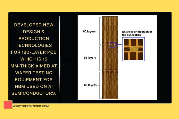
To overcome this, OTC developed two key technologies. The first is Sintering Paste for Via Bonding, a conductive-paste inter-substrate via-bonding process that lets multiple multilayer PCBs be stacked and electrically connected by joining the vias on their surfaces.
The second is a technology for manufacturing ultra-high-thickness PCBs up to 15 mm thick. By combining these, OTC has established design and production methods for proprietary 180-layer, 15 mm-thick PCBs made by stacking and connecting three 60-layer boards.
Using well-established techniques to manage via impedance, signal integrity, and power-supply behavior on each individual multilayer PCB, OTC can then stack them, achieving both ultra-high layer count and high performance and reliability.
This 180-layer PCB which is 15 mm-thick approach gives customers the signal and power quality needed to keep up with future requirements for high-speed, high-frequency, and high-density data transfer.
 OTC developed these technologies with high-growth fields in mind, including AI semiconductors, AI servers, aerospace and defense, and next?generation communications.
The company plans to keep evolving its PCB offerings and manufacturing know-how to stay aligned with ongoing advances in the industry.
OTC will be showcasing these technologies at PCB East 2026 (Booth 313), held at the DCU Convention Center in Worcester, Massachusetts, from April 28 to May 1, 2026.
To Know More: CLICK HERE
