


Kyocera Corporation has announced the commercialization of a new multilayer ceramic core substrate tailored for advanced semiconductor packages, including xPUs and switch ASICs that are scaling rapidly in complexity as AI data center architectures evolve. The new product will be unveiled at ECTC 2026, the International Conference on Electronic Components and Technology, in Orlando, Florida, from May 26–29, 2026.
Built from Kyocera’s proprietary Fine Ceramic materials, the core substrate is engineered for high-density wiring and exceptional rigidity.
According to the company, this combination dramatically reduces warpage in high-performance packages, an increasingly critical issue as demand for higher integration and faster processing continues to rise.
What is xPU?
The term “xPU” refers to a broad class of processing units, such as CPUs and GPUs, that handle AI-centric workloads and are often at the heart of accelerated computing platforms.
Key advantages of the new ceramic core
-
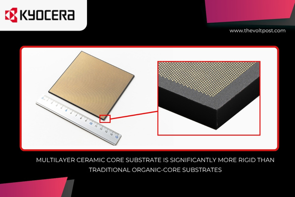
High rigidity, low warpage
The multilayer ceramic core substrate is significantly more rigid than traditional organic-core substrates, minimizing deformation throughout mounting and packaging steps.
This improved mechanical stability helps maintain fine-pitch interconnects and can enable higher device performance using thinner, more compact substrates.
-
Finer, denser wiring in three dimensions
In multilayer ceramic substrates, conductive paths between layers known as vias are formed while the ceramic is still pliable, before firing or sintering.
This enables smaller via diameters and tighter via pitches than conventional organic-core substrates, where vias are typically drilled.
The result is finer wiring and more compact, high-density 3D interconnects, which are essential for advanced AI and networking ASICs.
-
Custom design with upfront simulation support
Kyocera supports custom design requirements by providing thermal, electrical, and warpage simulations during the design phase, based on customer performance targets and specific assembly flows.
This simulation-driven approach helps customers converge faster on their design goals, reduce prototyping cycles, and increase yield in high-end packaging structures.
 A New AI-Era Packaging
The surge in generative AI and large language models is driving a global build-out of AI data centers, which in turn demands higher-performance xPUs and ASICs that rely on larger, more complex 2.5D packages.
In 2.5D packaging, multiple dies sit side-by-side on a high-density interposer, connected through fine wiring and vertical interlayers to boost bandwidth and speed.
Organic core substrates begin to run into limits at these scales: warpage, impedance control, and wiring-density constraints can bottleneck performance.
Kyocera’s multilayer ceramic core substrate addresses these pain points by combining higher rigidity, finer wiring, and tighter dimensional control making it a strong candidate for next?gen 2.5D and multi?chip modules in AI accelerators and network switches.
Kyocera says it will continue to expand its portfolio of advanced packaging materials based on laminated ceramic technology, targeting evolving requirements in high-performance computing, AI infrastructure, and networking ASICs.
To Know More: CLICK HERE
