


Taiwan Semiconductor Manufacturing Company (TSMC) is aiming to begin mass 3nm chip production in Japan by 2028, according to recent regulatory filings and government disclosures. The move centers on TSMC’s second fab in Kumamoto, where the company plans to upgrade the facility to run its most advanced logic node, marking Japan’s first domestic 3nm manufacturing capability.
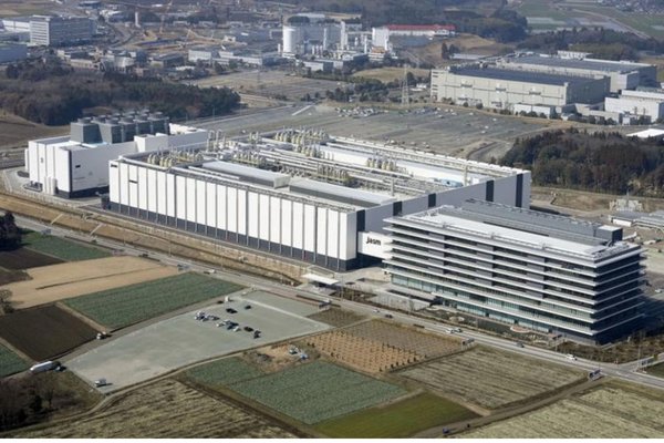
Under the revised plan, TSMC’s second Kumamoto facility will be equipped to produce around 15,000 12-inch wafers per month using the 3nm process. Equipment installation and mass production are both targeted to start in 2028, once construction and cleanroom work are complete.
This represents a major upgrade from the factory’s original scope, which focused on less?advanced 6nm-12nm technologies.
The 3nm chip production pivot at Kumamoto comes amid surging global demand for AI-accelerated computing, advanced smartphones, and high-performance data centers.
TSMC is positioning the Japan site as a key node in its international supply chain, helping customers secure cutting-edge capacity outside of Taiwan and reducing pressure on its main fabs.
Japan’s government and local partners, including Sony Semiconductor Solutions, have supported TSMC through incentives and joint-venture structures, seeking to strengthen the country’s semiconductor ecosystem and resilience.
The first Kumamoto fab, operated by Japan Advanced Semiconductor Manufacturing (JASM), began volume production in late 2024 using more mature nodes such as 12nm-28nm,

© Thomson Reuters
primarily serving automotive and industrial customers.
By scaling to 3nm in Japan, TSMC is not only deepening its overseas footprint but also aligning its technology roadmap with the needs of AI-driven markets.
