


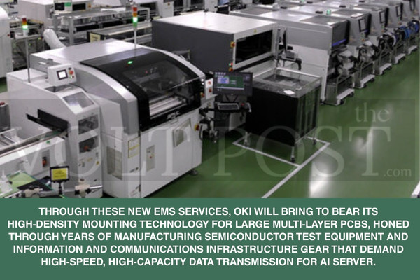
Through these new EMS services, OKI will bring to bear its high-density mounting technology for large multi-layer PCBs, honed through years of manufacturing semiconductor test equipment and information and communications infrastructure gear that demand high-speed, high-capacity data transmission for AI server.
OKI has launched a new Comprehensive Electronics Manufacturing Service (EMS) for AI server equipment, effective March 25, 2026.
The offering covers the full spectrum of production from design and fabrication of large-size, multi-layer PCBs using OKI’s proprietary high?heat?dissipation technology, optimized for high-speed, high-capacity data transmission, through component procurement, mounting, system assembly, testing, and rework. Targeting AI server makers, OKI is aiming for sales of ¥1 billion in FY2026.
As generative AI continues to accelerate, managing massive data volumes and securing enough computing power have become top priorities.
The compute needed for training and inference in generative AI can be hundreds of times greater than for traditional cloud services, driving strong demand for AI servers packed with dedicated AI chips such as GPUs and high-?bandwidth memory (HBM) for AI data centers.
AI server production lines face several tough challenges, achieving extremely high component placement accuracy, dealing with warping and interference from differing thermal expansion between PCBs and components during high-temperature heating, managing the intense heat generated by large numbers of AI chips in operation, and detecting hidden solder defects that AOI alone cannot catch.
Additional hurdles include expanding traceability requirements and increasingly complex rework on large, expensive AI semiconductors, all of which have contributed to lower yields, higher scrap-related costs, and longer lead times.
Through these new EMS services, OKI will bring to bear its high-density mounting technology for large multi-layer PCBs, honed through years of manufacturing semiconductor test equipment and information and communications infrastructure gear that demand high-speed, high-capacity data transmission.
It will also apply its simulation and manufacturing know-how for multi-layer boards using OKI’s proprietary embedded-copper-coin technology for superior heat dissipation.
Complementing these capabilities are OKI’s high-speed X-ray solder inspection, automated functional testing, and its high-mix, low-volume production expertise, all geared toward boosting yield and shortening time-to-market for AI servers.
On conventional lines, rework can be extremely difficult once semiconductors are mounted, especially for expensive, long-lead-time devices with fine-pitch packaging and high-density mounting.
 OKI has developed a dedicated rework line that combines proprietary jigs with the skilled handwork of its EMS technicians and advanced soldering techniques. This setup enables fast, reliable rework even on AI chips with over 10,000 pins, helping customers improve yields, reduce failure costs, shorten delivery times, and enhance overall production management efficiency.
To Know More: CLICK HERE
