



– Barley Li, Applications Engineering Manager – Technical Content, APAC, DigiKey
Satellite communications and radar systems increasingly require compact RF transmit chains that deliver high output power without overwhelming the platform’s size. This demand is especially critical in applications such as satellite payloads, SATCOM terminals, aerospace RF systems, and compact radar front ends, where output power must also be balanced against electrical efficiency and thermal constraints.
Achieving this balance gets increasingly difficult as operating frequencies approach 20 GHz. At K-band, RF designers cannot simply add gain and expect a practical transmit chain.
Conductor and package losses rise, and impedance matching becomes more sensitive. Furthermore, thermal density increases, while amplifier linearity limits usable output power long before a device reaches its saturated power rating.
Therefore, designers need power amplifiers that deliver watt-level RF output from milliwatt inputs, while reducing the integration burden on the surrounding RF front end. Bare-die or heavily customized implementations offer design flexibility, but they also raise the demands on assembly, matching, layout, and production repeatability.
Packaged monolithic microwave integrated circuit (MMIC) power amplifiers offer another route by integrating more of the RF power stage into a compact, manufacturable device.
However, squeezing watt-level RF power out of a chip that small concentrates a lot of power into a tiny area, and at roughly one-third efficiency, most of the DC the amplifier draws leaves as heat.
This heat, packed into a few square millimeters, drives up the junction temperature and can erode gain, efficiency, and reliability if left unmanaged.
Solving this problem falls to the amplifier’s semiconductor material. The material has to carry high power density while shedding the heat that it creates. GaN-on-SiC does both.
Gallium nitride’s high breakdown voltage enables operation at high voltage and high power density in a small die, and the silicon carbide substrate beneath it dissipates the concentrated heat away from the active region.
How the QPA1722 Supports Compact K-Band Transmit Chains
Qorvo offers a compact GaN-on-SiC amplifier that combines watt-level K-band output, high efficiency, and on-chip front-end integration.
The QPA1722 (Figure 1) is a high-power GaN MMIC power amplifier for RF front-end applications requiring watt-level output from 17.7 GHz to 20.2 GHz, making it a K-band power amplifier.
It sits at the antenna end of the transmit chain, after the driver and frequency-conversion stages, where the signal has to be strong enough to close a satellite link or return a radar echo, for example.
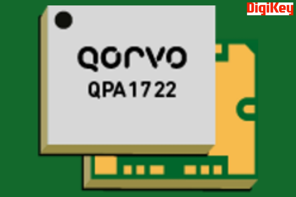
The device delivers 40 dBm (10 W) of saturated output power from a 22 dBm (roughly 160 mW) input. While saturated power defines the device’s maximum output, the linear figure matters more for communications.
The QPA1722 delivers 37 dBm (about 5 W) of linear output power. Modulated SATCOM waveforms exhibit high peaks, and exceeding the linear region causes spectral regrowth that spills energy into adjacent channels.
The 3 dB step from the 40 dBm ceiling down to the 37 dBm linear point gives designers tradeable headroom to keep the signal clean. Even so, linearity is moderate: two-tone IMD3 sits at -25 dBc at 34 dBm per tone, which dense modulation would pair with upstream back-off or digital predistortion.
The device also provides 26 dB of small-signal gain, reducing the amount of drive power required from preceding amplifier stages. This simplifies transmit-chain design by allowing the QPA1722 to provide a large share of the required power gain in a single packaged device.
Efficiency is another major design consideration. At 35% power-added efficiency, a meaningful share of the amplifier’s DC power is dissipated as heat, concentrated within a package millimeters across. Heat is unavoidable in K-band amplifiers.
However, the QPA1722 SATCOM power amplifier’s GaN-on-SiC construction carries it out of the active region, ensuring the amplifier sustains watt-level output without the thermal derating a less capable material would force.
The device also includes integration features to simplify RF front-end implementation. It is fully matched to 50 ? on both ports, eliminating the need for the lossy external matching you would otherwise design at K-band. The I/O ports are DC-grounded for ESD robustness, along with on-chip blocking capacitors that follow those DC grounds on the input and output.
An integrated power detector rounds out the on-chip features. It reports the output level for diagnostics, calibration, or closed-loop control without an external coupler, enabling system designers to monitor the system effectively. In RF systems where performance can shift with temperature, aging, operating mode, or antenna conditions, built-in detection can provide useful visibility into the transmit path.
The QPA1722 K-band power amplifier ships in a compact, surface-mount body measuring 6.0 mm × 5.0 mm × 1.64 mm. Its dimensions allow designers to fit watt-level K-band amplification into a space-constrained front end without stepping up to a larger module or a hybrid build.
Every part is 100% DC and RF tested against its electrical specifications, and the device is lead-free and RoHS-compliant, making it suitable for commercial and military communications.
Conclusion
As SATCOM and radar front ends move onto compact, constrained platforms, RF designers need practical ways to deliver watt-level transmit power at near-20 GHz without adding integration complexity.
Qorvo’s QPA1722 GaN power amplifier packages 10 W of K-band output, competitive efficiency, and on-chip matching and detection into a compact surface-mount MMIC, giving space-constrained front ends a full transmit stage in one part.
Source: DigiKey