


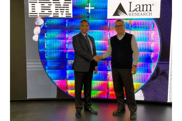
IBM and Lam Research are teaming up on a major five-year research push to crack sub-1nm logic chip tech, zeroing in on High-NA EUV lithography, cutting-edge materials, and 3D designs that are make-or-break for the AI boom.
IBM and Lam Research Chase Sub-1nm Breakthroughs
This builds on more than a decade of collaboration that powered early 7nm work, nanosheet transistors, and IBM’s groundbreaking 2nm chip back in 2021.
Now they’re doubling down on the tough stuff for sub-1nm nodes like etching, deposition, new materials, and High-NA EUV patterning.
The work will happen at IBM’s Albany NanoTech Complex, using Lam’s gear such as Aether dry resist, Kiyo/Akara etchers, Striker/ALTUS deposition tools, and packaging tech.
They’re aiming for complete process flows on nanosheet/nanostack devices with backside power delivery, all to nail high-yield manufacturing at these tiny scales.
Navigating 3D Scaling for AI
With traditional flat scaling running out of steam, the focus is shifting to intricate 3D structures for better performance, efficiency, and density.
IBM and Lam Research want to reimagine how lithography, materials, and processes work together as one system to deliver lower-power, high-performance transistors.
It’s all driven by exploding AI demands for tinier, greener logic nodes. This partnership puts them out front on High-NA EUV dry resist flows and next-gen interconnects.

Leadership Comments
IBM Semiconductor GM Mukesh Khare pointed to their history: “Lam’s been a key partner for over 10 years, helping with nanosheet and our first 2nm node. Excited to tackle High-NA EUV and sub-1nm hurdles together.”
Lam Research CTO Vahid Vahedi agreed: “In this 3D era, it’s all about meshing materials, processes, and lithography. Thrilled to push High-NA EUV advances with IBM for AI-ready transistors.”
Both stressed how this speeds up the path from lab to high-volume production, combining IBM’s research setup with Lam’s process know-how.
