


 SoC Designs in Chiplet-Based Architectures: Unlocking the Next Generation of Semiconductor Innovation
Executive Summary
The relentless demand for high-performance, low-power, and cost-efficient silicon is forcing a radical departure from traditional monolithic SoC designs. This white paper delves deep into the design principles and technical intricacies of SoC Designs using chiplet-based architectures.
It explores design partitioning strategies, interconnect protocols, power delivery mechanisms, thermal and mechanical challenges, along with detailed case studies. The paper also outlines the emerging ecosystem and implications for chip designers, foundries, and system integrators.
As of 2025, the chiplet paradigm has become the cornerstone for advanced computing, from AI accelerators to data center CPUs and mobile SoCs.
1. Introduction
With Moore’s Law slowing and design complexity exploding, chiplet-based architectures have emerged as a viable alternative. Instead of building large, monolithic SoCs on a single silicon die, the functionality is split into smaller dies (chiplets) that are assembled using advanced packaging. This modular approach not only improves yield but also allows for process heterogeneity, IP reuse, and faster design iterations.
These architectures offer multiple technical and economic advantages, including modular design, heterogeneous integration, design reusability, and improved manufacturability. Chiplet-based SoCs are particularly advantageous in high-performance computing (HPC), data center servers, mobile devices, and AI accelerators.
The momentum behind chiplet-based SoCs is bolstered by global investments, industry consortiums (such as UCIe and OCP), and the development of standardized interconnect protocols, advanced EDA tools, and sophisticated packaging technologies. As the semiconductor industry transitions from a transistor-scaling-centric paradigm to a system-scaling approach, chiplets are emerging as the architectural linchpin of next-generation silicon design.
2. Evolution of SoC Designs

2.1 Monolithic SoC Challenges
Historically, SoCs were fabricated on a single piece of silicon, which made design and integration relatively straightforward. However, as transistor sizes have decreased to sub-5nm nodes, the physical limitations of monolithic integration have become apparent:
- Yield Loss: The defect density per unit area remains constant or even increases in advanced nodes. Consequently, larger monolithic dies have a higher probability of defects, significantly lowering the effective yield. For example, at 5nm, a monolithic SoC greater than 600mm² may see yields drop below 40%.
- Power Density and Thermal Constraints: With all IP blocks integrated on one die, power density increases, creating thermal hotspots and limiting overall performance.
- Longer Time-to-Market: RTL-to-GDSII timelines for monolithic SoCs can stretch beyond 24 months, especially for complex designs with over 10 billion transistors.
- Higher NRE Costs: Mask costs alone at 3nm can exceed $25 million, making design reuse critical.

Comparison of Monolithic SoC vs. Chiplet-Based SoC
| Feature | Monolithic SoC | Chiplet-Based SoC |
|---|---|---|
| Die Size | Large, monolithic | Multiple smaller chiplets |
| Yield | Lower for large dies | Higher due to smaller dies |
| Process Node Flexibility | Single node for entire chip | Heterogeneous process nodes |
| Design Reuse | Limited | High |
| Time-to-Market | Longer due to monolithic complexity | Shorter due to modular design |
| Power Density | High, with thermal hotspots | Lower, distributed across chiplets |
| Cost | Higher NRE and mask costs | Lower per chiplet, but assembly cost added |
| Scalability | Limited | Highly scalable |
2.2 Chiplet-Based Paradigm
In contrast, chiplet-based architectures offer a compelling alternative by disaggregating functionality into smaller, independently manufactured dies. These chiplets are then assembled into a single package to deliver holistic system functionality.
- Functional Partitioning: Compute, memory, I/O, analog, and security modules can be implemented as separate chiplets.
- Process Technology Heterogeneity: Designers can use the latest node (e.g., 3nm) for compute-intensive chiplets, while using mature nodes (e.g., 16nm or 28nm) for analog, RF, or I/O chiplets.
- IP Reusability and Faster Time-to-Market: Existing IP blocks can be reused across products, shortening development cycles.
This paradigm also promotes scalability, allowing manufacturers to tailor the number and type of chiplets according to different market segments.
3. Chiplet-Based SoC Architecture
3.1 Architectural Partitioning
A chiplet-based SoC can be designed using several architectural partitioning strategies:
- Horizontal Partitioning: Different functions are separated into horizontally laid out chiplets. Examples include CPU chiplets, GPU chiplets, HBM modules, and I/O controllers.
- Vertical Partitioning (3D Integration): Stacking chiplets vertically offers higher bandwidth and lower latency between components, especially between memory and compute units.
The choice of partitioning affects not only performance but also signal integrity, power delivery, and thermal behavior.
3.2 Clock and Reset Domain Management
Managing clocks across multiple chiplets is a significant design challenge:
- Independent PLLs: Each chiplet may generate its own clock using on-chip Phase-Locked Loops (PLLs), with clock alignment performed using handshake and synchronization protocols.
- CDC Protocols: Robust Clock Domain Crossing protocols are necessary to ensure metastability is mitigated across chiplet boundaries.
- Reset Management: Global and local resets must be coordinated to ensure correct system initialization.
4. Interconnect Technologies
Interconnect Protocols for Chiplet Architectures
| Protocol | Data Rate per Lane | Signaling Type | Typical Use Case | Standardization Status |
|---|---|---|---|---|
| UCIe (Universal Chiplet Interconnect Express) | 16–64 GT/s | Electrical (SerDes PAM4) | High-performance CPU/GPU chiplets | Industry standard, consortium-backed |
| BoW (Bunch of Wires) | Up to 10 GT/s | Electrical (NRZ) | Low power, cost-sensitive applications | Open Compute Project (OCP) supported |
| OpenHBI (Open High-Bandwidth Interface) | 20+ GT/s | Electrical | 3D stacking, memory interfaces | Emerging, experimental |
| EMIB (Embedded Multi-die Interconnect Bridge) | Up to 20 GT/s | Electrical | Intel’s high-density interposer-based chiplets | Proprietary by Intel |
4.1 Electrical Interconnects
The backbone of a chiplet-based SoC is its interconnect fabric:
- UCIe (Universal Chiplet Interconnect Express): A standardized die-to-die interconnect protocol supporting 16–64 GT/s per lane. It includes PHY, link, transport, and protocol layers. UCIe is emerging as the Ethernet of chiplets.
- BoW (Bunch of Wires): Developed by the Open Compute Project, BoW supports cost-effective, low-power interconnects.
- OpenHBI: High-Bandwidth Interface optimized for 3D stacking and dense chiplet interconnects.
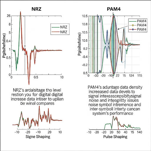
4.2 Signaling Techniques
- SerDes Links: High-speed serial links using either NRZ (Non-Return-to-Zero) or PAM4 (Pulse Amplitude Modulation with 4 levels). PAM4 offers higher data rates but demands better signal integrity management.
- Silicon Interposers and Organic Substrates: Support dense wiring and signal routing across chiplets.
4.3 Latency and Bandwidth Considerations
- Interconnect latency can range from sub-nanoseconds (for 3D bonded chiplets) to tens of nanoseconds (for 2.5D and substrate-based links).
- Bandwidth is determined by lane count, encoding, and signaling method.
5. Power Delivery and Management
Power Delivery Techniques in Chiplet SoCs
| Technique | Description | Benefits | Challenges |
|---|---|---|---|
| Dedicated VRMs per Chiplet | On-package/on-die voltage regulators | Tailored power supply per chiplet | Increased design complexity |
| Package-Level Decoupling | Capacitors close to chiplets reduce noise | Improves power integrity | Adds to package complexity |
| Dynamic Voltage and Frequency Scaling (DVFS) | Per-chiplet DVFS controls power/performance | Energy efficiency | Requires complex coordination |
| Power Gating | Power down inactive chiplets | Saves leakage power | State retention overhead |
5.1 Power Delivery Network (PDN)
Each chiplet may require dedicated voltage domains and regulation circuitry:
- Dedicated VRMs (Voltage Regulator Modules): On-package or on-die voltage regulation tailored to each chiplet’s power profile.
- Package-Level Decoupling: Advanced packaging integrates decoupling capacitors closer to chiplets for noise suppression.
- Power Integrity Simulations: Simulate PDN impedance and IR drop across chiplets to ensure robust operation.
5.2 DVFS and Power Gating
- Fine-grained Dynamic Voltage and Frequency Scaling (DVFS) per chiplet improves energy efficiency.
- Clock gating and power gating techniques isolate idle chiplets.
6. Thermal and Mechanical Design
6.1 Thermal Management
- Active and Passive Cooling Solutions: Use vapor chambers, microfluidic cooling, and finned heat sinks.
- Thermal Simulations: CFD (Computational Fluid Dynamics) tools are used for package-level thermal simulation.
- Hotspot Management: Algorithms redistribute workloads based on thermal profiles.
6.2 Mechanical Integrity
- Warpage Control: Controlled Coefficient of Thermal Expansion (CTE) matching in substrates and encapsulants reduces package warpage.
- Stress Modeling: Finite Element Analysis (FEA) used to model stress due to package assembly and thermal cycling.
7. Packaging and Integration
Packaging Technologies in Chiplet Integration
| Packaging Type | Description | Advantages | Typical Use Cases | Limitations |
|---|---|---|---|---|
| 2.5D Integration (Silicon Interposer) | Chiplets mounted on silicon/glass interposer with micro-bumps and TSVs | High bandwidth, lower latency | HBM memory integration, logic stacking | Costly, complex manufacturing |
| 3D Stacking (Face-to-Face, Hybrid Bonding) | Vertical stacking of chiplets with fine-pitch interconnects | Minimal footprint, ultra-low latency | High-performance CPUs, GPUs | Thermal management complexity |
| Fan-Out Wafer-Level Packaging (FOWLP) | Redistribution layers for routing in package | Low parasitic capacitance, good thermal performance | Mobile SoCs (Apple, Qualcomm) | Limited vertical stacking |
7.1 2.5D Integration
- Silicon or glass interposers with micro-bumps.
- TSVs (Through-Silicon Vias) used for inter-chiplet communication.
- Ideal for HBM and logic stacking.
7.2 3D Stacking
- Face-to-Face and Back-to-Face bonding.
- Hybrid bonding enables <10µm pitch interconnects.
- Reduces latency, increases bandwidth, and minimizes footprint.
7.3 Fan-Out Wafer-Level Packaging (FOWLP)
- Redistributed Layers (RDL) used for signal routing.
- Enhanced thermal dissipation and lower parasitics.
- Examples: Apple A-series and Qualcomm Snapdragon.
8. Validation and Testing
Key EDA Tool Requirements for Chiplet-Based SoC Design
| Tool Category | Requirements Specific to Chiplet SoCs | Example Tools / Vendors |
|---|---|---|
| RTL Design & Partitioning | Support for modular IP blocks and interface definitions | Cadence Innovus, Synopsys Fusion Compiler |
| Physical Design & Floorplanning | Multi-die floorplanning, co-placement of chiplets | Synopsys IC Compiler, Cadence Encounter |
| Signal Integrity & Timing Analysis | Cross-die timing closure, inter-chiplet link modeling | Ansys HFSS, Cadence Sigrity |
| Power Integrity Analysis | Multi-domain PDN modeling and package-level power analysis | Ansys RedHawk, Siemens Simcenter |
| Verification & Validation | Multi-clock domain CDC analysis, inter-chiplet protocol verification | Mentor Questa, Cadence JasperGold |
| Thermal & Mechanical Simulation | CFD and FEA co-simulation of package and thermal behavior | ANSYS Fluent, COMSOL Multiphysics |
8.1 Known Good Die (KGD)
- KGDs are pre-tested chiplets that pass wafer-level burn-in.
- Minimizes integration failure and improves overall package yield.
8.2 System-Level Testing
- Boundary Scan using IEEE 1149.1/1149.6.
- Built-In Self-Test (BIST) mechanisms for inter-chiplet links.
- Test Access Mechanism (TAM) routing via interposers.
8.3 Power and Thermal Validation
- Power modeling using tools like Ansys RedHawk.
- Thermal profiling via IR thermography.
- Electrothermal co-simulation integrates power and temperature analysis.
9. Real-World Implementations
9.1 AMD
- EPYC and Ryzen families use chiplets for CPU cores and I/O die.
- Infinity Fabric provides coherent interconnect across chiplets.
9.2 Intel
- Meteor Lake: Combines compute, GPU, and SoC tile using Foveros.
- Ponte Vecchio GPU: Uses over 47 chiplets connected via EMIB and Foveros.
9.3 Apple
- M1 Ultra: Combines two M1 Max SoCs via UltraFusion interconnect (2.5TB/s).
9.4 TSMC
- CoWoS: Chip-on-wafer-on-substrate platform supporting up to 12 chiplets.
- SoIC: Enables hybrid bonding at ultra-fine pitch.
10. Design Automation Tools for Chiplet SoCs
10.1 EDA Toolchain Requirements
Electronic Design Automation (EDA) tools for chiplet-based SoCs must support hierarchical design, heterogeneous integration, and advanced packaging features. Traditional monolithic SoC flows are not sufficient for chiplet systems due to multi-die management and packaging complexity.
- Physical Design Tools: Must support multi-die floorplanning, thermal-aware placement, and cross-die routing.
- Signal Integrity and Timing Analysis: Required to manage die-to-die interconnect timing closure, skew compensation, and jitter management.
- Thermal-Aware Design Tools: Integrated thermal simulation with layout to anticipate hotspots.
- Co-Simulation Engines: Cross-domain simulation (power, thermal, mechanical, timing) across multiple chiplets.

10.2 Co-Design and Co-Verification
- System-Level Co-Design: Tools like Cadence Integrity 3D-IC or Synopsys 3DIC Compiler allow cross-domain co-design of chiplets, interposers, and packages.
- Package-Aware Simulation: Incorporates electrical parasitics and package-level interactions in RTL simulation.
- Multi-Die DFT Integration: Design-for-test tools need to stitch together test strategies across chiplets using standardized TAPs (Test Access Ports).
10.3 Hardware/Software Co-Verification
- Virtual Prototyping: Early software development on virtual models of chiplet SoCs enables parallel HW-SW development.
- Firmware-Aware Emulation: Tools that simulate firmware-hardware interactions across chiplets ensure robust boot flows and inter-chiplet orchestration.
10.4 Design Standards
- IEEE P1838: Standard for test access architecture for 3D stacked ICs and chiplet-based integration.
- UCIe 1.1/2.0 Integration: Tool support for UCIe protocol stack ensures correct link layer behavior and power state transitions.
11. Security Implications in Chiplet Architectures
11.1 Security Challenges
Chiplet-based SoCs introduce new attack surfaces due to multiple die integration and inter-chip communication channels. Key challenges include:
-
Supply Chain Risks: Sourcing chiplets from multiple vendors increases the risk of counterfeit or malicious IP insertion.
-
Inter-Chiplet Communication Security: Data traveling over interconnects like UCIe can be intercepted or tampered with.
-
Isolation and Trust: Ensuring secure isolation between chiplets with different trust levels is complex.
11.2 Hardware Security Techniques
-
Secure Boot and Chain of Trust: Each chiplet must support secure boot mechanisms, validated through hardware root-of-trust anchors.
-
Encrypted Interconnects: Employing on-die or package-level encryption protocols to protect data on chiplet interconnects.
-
Physical Unclonable Functions (PUFs): Unique silicon fingerprints embedded in chiplets for authentication and anti-counterfeiting.
-
Side-Channel Attack Mitigation: Careful power and electromagnetic leakage analysis across chiplet boundaries.

11.3 Design-for-Security (DfS) Strategies
-
Partitioning Security Domains: Grouping chiplets by security levels to contain potential breaches.
-
Runtime Monitoring: On-chip monitors track anomalies in chiplet behavior or communication.
-
Hardware Root-of-Trust Management: Centralized or distributed secure elements embedded in chiplets to enforce security policies.
12. Ecosystem and Standardization Efforts
12.1 Industry Consortiums
-
Universal Chiplet Interconnect Express (UCIe): Industry-wide standard to enable interoperable chiplets from different vendors, with wide backing from AMD, Intel, TSMC, and others.
-
Open Compute Project (OCP) and BoW: Promoting open standards for chiplet interconnects with cost-effective, energy-efficient solutions.
-
JEDEC and IEEE: Defining packaging, test, and security standards for chiplet modules.
12.2 Supply Chain and IP Reuse
-
IP marketplaces for certified chiplets are emerging, enabling designers to rapidly assemble SoCs.
-
Verified IP and chiplet catalogs ensure trust and accelerate integration.
12.3 Packaging and Foundry Partnerships
-
Foundries are offering integrated CoWoS, SoIC, and Foveros services that include chiplet manufacturing and advanced packaging.
-
EDA tool vendors collaborate closely with packaging houses to offer end-to-end design flows.
13. Future Trends in Chiplet-Based SoCs
13.1 Integration of Heterogeneous Architectures
-
Increasing integration of RISC-V, AI accelerators, GPUs, and analog/RF chiplets tailored for specialized workloads.
-
More mature use of 3D stacking with hybrid bonding at sub-10µm pitch scales.
13.2 Optical Interconnects
-
On-package optical interconnects promise to overcome electrical signaling limits with higher bandwidth and lower latency.
-
Research is ongoing on integrating silicon photonics chiplets with electrical compute chiplets.
13.3 AI-Driven Design Automation
-
Machine learning algorithms optimize chiplet partitioning, floorplanning, and interconnect routing.
-
Predictive thermal and power modeling accelerates design cycles.
13.4 Secure and Trustworthy Chiplets
-
Adoption of zero-trust hardware architectures.
-
Increasing use of formal verification methods for chiplet IP.
13.5 Standardized Chiplet Verification and Certification
-
Industry moves towards universal chiplet certification frameworks to ensure interoperability and quality.
14. Conclusion
Chiplet-based SoC architectures represent a transformative evolution in semiconductor design, breaking through the limitations of monolithic integration. By enabling modular, heterogeneous, and scalable system construction, chiplets unlock new frontiers in performance, cost-efficiency, and time-to-market. The challenges of interconnect design, power delivery, thermal management, security, and ecosystem integration are being met through rapid technological advances, industry collaboration, and new standards.
As of 2025, chiplets are central to cutting-edge products spanning AI, HPC, mobile, and IoT, and their role will only deepen as optical interconnects, advanced packaging, and AI-driven design automation mature. Embracing the chiplet paradigm allows semiconductor designers and manufacturers to navigate Moore’s Law slowdowns and sustain innovation in an increasingly complex silicon landscape.
15. References
-
Universal Chiplet Interconnect Express (UCIe) Specification, UCIe Consortium, 2023.
-
“Chiplet-Based Design: Revolutionizing SoC Development,” IEEE Spectrum, 2024.
-
TSMC CoWoS and SoIC Technology Overview, TSMC White Paper, 2023.
-
“3D-IC and Advanced Packaging: Challenges and Solutions,” Cadence Design Systems, 2024.
-
“Security in Chiplet-Based Architectures,” Synopsys Technical Brief, 2024.
-
AMD EPYC Chiplet Architecture White Paper, AMD, 2022.
-
Intel Foveros Technology Overview, Intel Corp., 2023.
-
“EDA for Chiplet Systems: New Challenges and Tools,” DAC Conference Proceedings, 2024.
-
Open Compute Project (OCP) Bunch of Wires (BoW) Specification, 2023.
-
“Optical Interconnects in Chiplet SoCs,” Journal of Lightwave Technology, 2024.
