


Union Minister for Electronics & Information Technology, Railways, and Information & Broadcasting, Shri Ashwini Vaishnaw, inaugurated India’s first 3nm chip design centres in Noida and Bengaluru.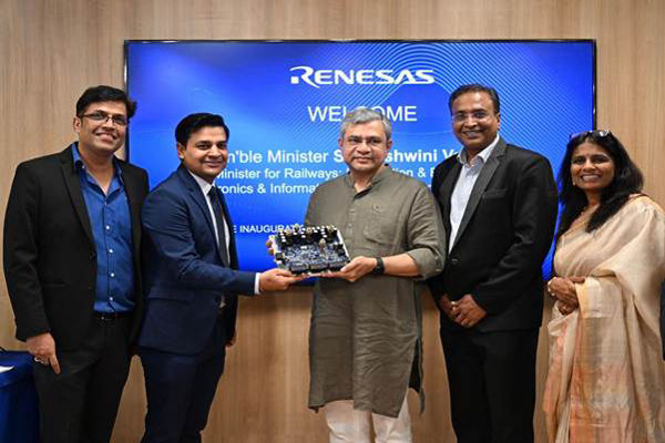
These state-of-the-art facilities, established by Renesas Electronics India Private Limited, mark a significant leap in India’s semiconductor capabilities, positioning the nation among global leaders in advanced chip design.
A Step Towards Becoming Global Semiconductor Hub
The launch of these 3nm chip design centres underscores India’s commitment to becoming a global semiconductor hub. Minister Vaishnaw highlighted the nation’s holistic semiconductor strategy, encompassing design, fabrication, Assembly, Testing, Marking, and Packaging (ATMP), equipment, chemicals, and gas supply chains.
He emphasized the growing confidence of global investors, citing significant investments by companies like Applied Materials and Lam Research.
“Designing at 3nm is truly next-generation. We’ve done 7nm and 5nm earlier, but this marks a new frontier,” the Minister stated, emphasizing the importance of this development in India’s semiconductor journey.
Empowering Future Engineers
To further strengthen the semiconductor ecosystem, the government announced the launch of a new semiconductor learning kit aimed at enhancing practical hardware skills among engineering students.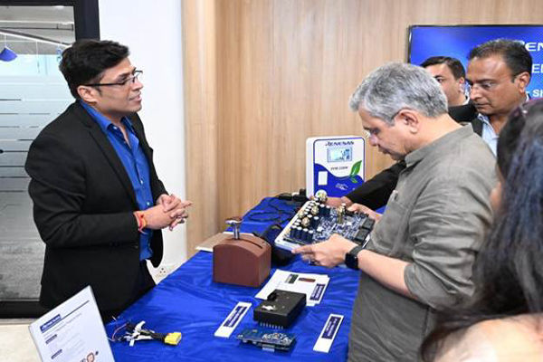
Over 270 academic institutions, already equipped with advanced Electronic Design Automation (EDA) software tools under the India Semiconductor Mission, will receive these hands-on hardware kits. This initiative aims to create industry-ready engineers by integrating software and hardware learning.
Minister Vaishnaw praised the efforts of the Centre for Development of Advanced Computing (CDAC) and the India Semiconductor Mission (ISM) team for their efficient execution, reaffirming the government’s commitment to nurturing India into a global semiconductor leader.
Industry Collaboration and Global Partnerships
Hidetoshi Shibata, CEO & MD of Renesas Electronics, expressed the company’s commitment to expanding end-to-end semiconductor capabilities in India, from architecture to testing. He highlighted India’s strategic importance, citing the nation’s growing contributions in embedded systems, software, and system innovation.
Renesas aims to support over 250 academic institutions and numerous startups through government-backed initiatives like the Chips to Startup (C2S) Programme and the Design Linked Incentive (DLI) Scheme.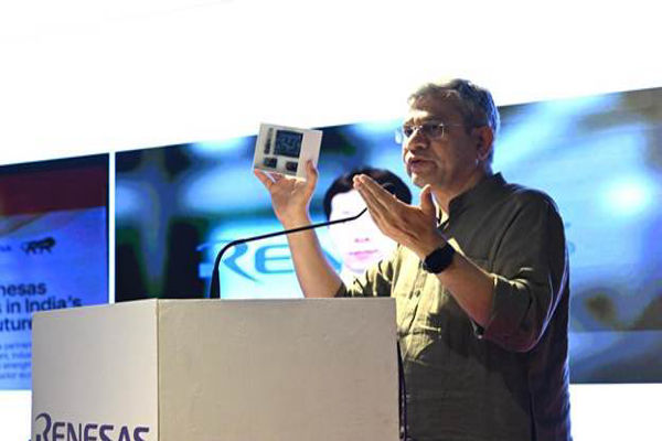
“India’s talent strength and shared Indo-Japan strategic interests will help reinvent the global semiconductor lifecycle,” Shibata stated, emphasizing the potential of this collaboration in shaping the future of the semiconductor industry.
