


OKI Circuit Technology has successfully developed 124-layer PCB technology for wafer inspection equipment built for next-generation high bandwidth memory, such as HBM (Note 1), which is installed on AI semiconductors.
This is a 15% increase in the number of layers over traditional 108-layer designs. OTC plans to establish mass production technology at its Joetsu Plant in Joetsu City, Niigata Prefecture, by October 2025. The plant has a proven track record and advanced development and production capabilities in the field of high multilayer, high-precision, large-format PCBs for semiconductor inspection equipment.
AI computing necessitates massive data transfers between graphics processing unit (GPU) semiconductors and memory.
As semiconductor performance improves, the memory installed must be able to transfer data at high speeds, frequencies, and densities.
HBM has a layered DRAM (Note 2) structure, which necessitates technology capable of producing wafers even thinner and more precisely. This arrangement necessitates that the PCBs used in inspection equipment achieve even greater levels of performance and quality.
Because modern semiconductors handle a large amount of signals and the number of wafer-mounted chips increases as a result of process downsizing, it is required to improve density and layer count on the PCBs used in inspection equipment.
However, due to numerous limits, PCB thickness has been limited to 7.6 mm, with 108 layers being the highest limit with conventional technology.
This time, OTC has successfully developed 124-layer PCB technology with a board thickness of 7.6 mm by developing ultra-thin materials, tools, and handling technologies, as well as developing and introducing a proprietary automatic transport system for ultra-thin materials into its manufacturing line.
OKI is actively engaged in its EMS business, which is built on the basic concept of delivering comprehensive manufacturing services ranging from design to production and testing.
OKI maintains a strong emphasis on technological development in the PCB industry, and this new technology was created in response to industries predicted to experience future growth, such as AI semiconductors, aerospace, defense, robots, and next-generation communications.
OKI will continue to develop PCBs and manufacturing technologies in response to future technological advancements.
PCB East 2025
To demonstrate this technology, OTC will exhibit at the OTC booth (No.305) at PCB East 2025, which will take place from April 30 to May 2, 2025, at the Boxboro Regency Hotel and Conference Center in Massachusetts, USA.
Note 1: HBM (High Bandwidth Memory)
Next-generation high-bandwidth memory. Consists of multiple stacked DRAM with a dedicated high-speed interface.
Note 2: DRAM (Dynamic Random Access Memory)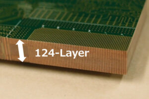
A type of temporary data storage memory widely used in computers and electronic devices, made up of cells consisting of capacitors that hold electric charge and transistors to control this charge. As volatile memory, this memory loses data when power supply is cut off. In addition, it allows for high-speed data read/write and is well-suited for increased capacity. It is used in personal computers, servers, mobile devices, etc.
For Further Info, CLICK HERE
