





Microchip Technology has introduced the SY757xx family of 1.2V-output LVCMOS clock buffers, targeting the growing demand for low-voltage clock solutions in high-performance FPGAs, SoCs, AI accelerators and next-generation CPUs.
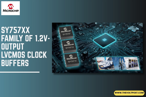
The new clock buffers are designed to simplify board design while maintaining signal integrity and ultra-low additive jitter. They address a growing challenge for PCB designers working with advanced FinFET-based devices, where standard 1.2V LVCMOS clock buffers and level-translating solutions can be difficult to source.
Traditional designs often rely on discrete components and voltage-divider circuits to convert higher-voltage clock signals to the lower levels required by modern devices. While these approaches can work, they can also add components and board complexity while introducing risks such as signal degradation and clock duty-cycle distortion.
Microchip’s SY757xx family is designed to remove much of that complexity by providing the required clock buffering and voltage translation in a single device.
The family supports a broad range of supply voltages and operating frequencies, giving designers greater flexibility when working with legacy board power supplies and different clock-source voltage levels. The devices support clock distribution with additive jitter as low as 26 femtoseconds, while covering frequencies from 0 Hz to 250 MHz.
Designed for High-Speed Computing Platforms
As semiconductor processes become increasingly advanced, maintaining clean and accurate clock signals is critical for high-speed computing platforms.
The SY757xx devices are aimed at FPGA, SoC and CPU applications where low latency, high-speed parallel processing, hardware reconfigurability and real-time computing are essential. Potential applications include embedded vision and video processing, AI and machine learning acceleration, industrial control, IoT, networking and communications, signal processing and embedded systems.
The devices are also designed to support clock fanout and distribution while maintaining the resolution and signal integrity required by these demanding platforms.
Multiple Configurations and Packages
Microchip is launching three SY757xx devices in volume production, while another eight devices are currently sampling in limited volumes. The portfolio covers multiple configurations and is available in three space-saving package options.
The family includes solutions capable of translating clock signals across a 1.2V to 3.3V input range, including a single-chip option for connecting 3.3V components to FPGAs and SoCs that require a 1.2V clock signal.
Compared with discrete-component solutions, the integrated buffers can reduce component count and bill-of-materials costs while helping designers optimise AC coupling and biasing. They can also help avoid the design-margin and duty-cycle distortion issues that can occur with discrete voltage-divider circuits.
Production Devices and Pricing
Three devices are currently in volume production. The SY75707TWL-TR supports a differential input and two LVCMOS outputs and is housed in an 8-pin Very-thin Dual Flat No-lead (VDFN) package.
The SY75712TWL-TR and SY75714TWL-TR provide two and four LVCMOS outputs, respectively, operating at 1.2V to 1.8V rails. Both are available in 8-pin Thin Dual Flat No-lead (TDFN) packages.
Pricing ranges from $0.50 to $0.83 per unit, depending on configuration, based on quantities of 10,000 units.
The remaining eight SY757xx devices support 1.2V to 1.8V LVCMOS outputs and offer a choice of single-ended 1.2V to 3.3V LVCMOS inputs, single-ended 1.2V to 1.8V LVCMOS inputs or differential 1.8V to 3.3V inputs. The portfolio also includes an output-enabled fanout buffer option. All sampling devices are housed in 8-pin VDFN packages.
Part of Microchip’s Broader FPGA and SoC Portfolio
The SY757xx family complements Microchip’s portfolio of flash-based FPGAs and SoC FPGAs, which spans ultra-low-density through mid-range devices.
The company also offers microcontrollers, analog components, power management, timing, connectivity and memory products. These devices are designed to work together as part of a broader system approach, helping engineers simplify development and reduce design risk across increasingly complex electronic platforms.
Key Comment
 “Our SY757xx family of clock buffers helps customers overcome the growing clock distribution challenges associated with next-generation high-performance FPGA, SoC and CPU platforms,” said Maamoun Abou Seido, appointed vice president of Microchip’s timing and communications business unit. “By combining ultra-low additive jitter performance with broad VDD and wide frequency support in a single-chip solution, the SY757xx devices simplify board design, reduce component count and help customers maintain the signal integrity and timing accuracy required in today’s high-performance computing applications.”
For additional information and to purchase, contact a Microchip sales representative, authorized worldwide distributor or visit Microchip’s Purchasing and Client Services website, www.microchipdirect.com.
For information about SY757xx products that are available in sample volumes, email tcghelp@microchip.com.