


Renesas Electronics just unveiled three breakthrough System-on-Chip (SoC) technologies for next-gen automotive multi-domain ECUs. These pack advanced AI processing and chiplet capabilities, forming the backbone for software-defined vehicles (SDVs). The company shared the details at the International Solid-State Circuits Conference (ISSCC 2026) in San Francisco, February 15–19.
In the SDV era, automotive SoCs need to juggle tons of apps at once, scale via chiplets, and hit top functional safety marks like ASIL D.
But as these chips grow bigger and more complex, keeping quality high while curbing power use gets tricky. Renesas tackled this head-on with some clever innovations.
Chiplet Design That Nails Functional Safety
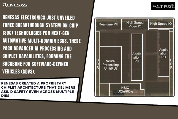
Renesas created a proprietary chiplet architecture that delivers ASIL D safety even across multiple dies. They paired the standard UCIe die-to-die interface with a custom RegionID system to block resource interference when apps run wild achieving true Freedom from Interference (FFI).
Traditional UCIe couldn’t pass RegionIDs between dies, so Renesas mapped them into the physical address space, encoded them for UCIe transmission, and locked down access via MMU and real-time cores.
Tests clocked it at 51.2 GB/s near the max for on-chip speeds proving scalability without sacrificing safety.
Beefed-Up AI with Automotive Reliability
For SDV-grade quality, Renesas built a 3 nm SoC that supercharges neural processing units (NPUs) for AI tasks. NPUs have ballooned in size (1.5x bigger than before), spiking clock latency from shared sources.
Ditch module-level clock pulse generators (CPGs) for mini-CPGs (mCPGs) placed right at the sub-module level, slashing latency to meet strict timing.
To handle testing headaches from this layered setup crucial for zero-defect automotive chips they wove in test circuits, unified clock paths, and synced everything under one source in test mode. Result: Rock-solid reliability for massive SoCs.
Smarter Power Control for Efficiency and Safety
Renesas rolled out advanced power gating across 90+ domains, dialing control from milliwatts to tens of watts based on workload.
They split power switches into ring and row types to fight IR drops from shrinking process nodes ring PSWs tame startup surges, row PSWs balance impedance, cutting drops by 13%.
For ASIL D, dual core lockstep (DCLS) uses separate power switches per master/checker core to catch failures. Gate signal loopback spots OFF-state issues, and a drift-resistant digital voltage meter (DVMON) boosts aging tolerance by 1.4 mV. It’s high performance with top efficiency and safety.
