




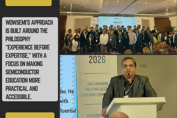
WOWSemi’s approach is built around the philosophy “Experience Before Expertise,” with a focus on making semiconductor education more practical and accessible.
As India accelerates its semiconductor ambitions, industry leaders and experts are calling for greater collaboration between education and industry to ensure the country has the skilled workforce needed to support the sector’s growth.
On Teachers’ Day, semiconductor professionals and industry stalwarts including PVG Menon, Suraj Rengarajan, Hanish Kumar, Arvind Ragunathan and Venkatesh Kumar Pandurengan came together to support the WOWSemi Foundation’s vision of creating an industry-ready semiconductor talent pool in India.
A key concern highlighted during the gathering was the gap between classroom learning and real-world industry experience. While India is investing heavily in semiconductor design and manufacturing capabilities, industry leaders believe students also need meaningful exposure to the technologies, processes and environments they will encounter in the workplace.
“India’s semiconductor opportunity is not just about building fabs; it is about building the people who will run them, innovate in them and take the ecosystem forward. The time to act is now,” said Venkatesh Pandurengan, highlighting the need to give young talent greater exposure to the industry.
The message carried particular significance on Teachers’ Day, underscoring the role educators can play in preparing students for a rapidly developing semiconductor ecosystem. As the sector expands, closer collaboration between academia and industry will be critical to developing engineers and technicians with both theoretical knowledge and practical experience.
Taking Semiconductor Learning Beyond the Classroom
WOWSemi’s approach is built around the philosophy “Experience Before Expertise,” with a focus on making semiconductor education more practical and accessible.
Through initiatives including Fab On Wheels, WOW Academy, WOW Semuseum, WOW Bot, Semipreneur and Green Fab City, students and aspiring engineers can gain exposure to semiconductor wafers, packages, equipment and manufacturing processes, along with virtual fabs, AI-enabled learning and other industry-relevant skills.
The initiatives have received support from industry leaders who see hands-on exposure as an important part of preparing India’s future semiconductor workforce. The concern is that India should not create another generation of engineers who understand semiconductor theory but have never experienced the working environment of a fab.
The broader sentiment from participating leaders was that India already has several of the ingredients needed to build a strong semiconductor ecosystem.
“India has the infrastructure ambition, the talent and the market. What we need now is a connected ecosystem where industry, academia and young minds work together,” was the collective sentiment expressed by the participating leaders.
Building a Semiconductor Talent Pipeline
WOWSemi aims to reach 5 lakh citizens across 11 states, 60 districts and 3,000 institutions by 2031, with a target of 1 lakh certifications. The initiative is intended to help create a broad-based talent pipeline capable of supporting India’s semiconductor ambitions.
 The gathering also reinforced a larger message: building fabs and expanding semiconductor infrastructure is only one part of the equation. India will also need people with the practical skills and experience to operate facilities, develop technologies and drive the ecosystem forward.
The chip may be tiny, but its potential impact on India’s economy is enormous. Turning that potential into reality will require more than technology and investment, it will require skills, experience, collaboration and a generation prepared to lead.
For WOWSemi, the vision can be summed up in three words:
Experience. Engineer. Empower.