


Setting a new benchmark in the semiconductor and memory technology landscape, Cadence Design Systems has unveiled the industry’s first memory IP for LPDDR6/5X running at speeds of up to 14.4Gb/s.
This advancement positions Cadence at the forefront of next-generation mobile, automotive, and AI computing solutions, marking a major milestone for performance and power efficiency.
Breaking the Speed Barrier with LPDDR6/5X
Cadence’s newly introduced IP delivers support for both LPDDR6 and LPDDR5X standards and achieves unprecedented data rates of 14.4Gb/s.
With this, it sets a new industry benchmark for memory interfaces, catering to bandwidth-intensive applications that are driving the future of edge computing, smartphones, automotive electronics, AR/VR systems, and AI accelerators.
The solution includes a complete memory interface subsystem: the PHY (physical layer), controller, and verification IP. Together, these components offer a comprehensive, low-power, and highly optimized design environment for system-on-chip (SoC) developers targeting sub-3nm process nodes.
Optimized for Advanced Nodes and AI Workloads
The IP is optimized for implementation on leading-edge foundry processes, particularly 3nm and below, ensuring that it aligns with the demands of AI and high-performance mobile applications.
With built-in support for dynamic voltage and frequency scaling (DVFS), the LPDDR6/5X memory IP helps reduce power consumption during low activity periods, while ramping up performance seamlessly when needed.
Cadence emphasized that the memory IP also enhances latency performance and reduces die area, giving chipmakers a powerful new tool for high-density system designs.
Enabling Next-Gen Applications
As AI and data-intensive applications continue to push the boundaries of memory performance, Cadence’s new IP comes at a critical time.
Automotive OEMs, hyperscalers, and mobile device manufacturers can now develop products that are faster, more efficient, and better equipped to handle growing computational demands.
This innovation is particularly relevant for electric and autonomous vehicles, where real-time data processing and safety-critical systems require ultra-high-speed memory access with minimal latency and energy usage.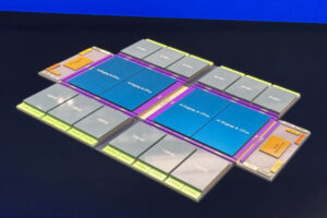
Integrating the LPDDR6/5X 14.4Gb/s IP into Chip design
Early access customers are already integrating the LPDDR6/5X 14.4Gb/s IP into their upcoming chip designs.
Cadence has also made the IP compatible with major DRAM vendors’ memory components, helping ensure rapid adoption across multiple platforms.
According to Cadence, its deep collaboration with key industry stakeholders and continuous focus on delivering cutting-edge EDA tools and IP solutions has enabled this breakthrough.
The company’s commitment to accelerating design innovation is reflected in this launch, which is expected to pave the way for the next generation of memory-centric computing.
Cadence’s unveiling of the industry’s first LPDDR6/5X memory IP at 14.4Gb/s is more than a technical achievement—it is a signal of what’s to come in the era of AI-optimized, high-performance systems.
