


TSMC and Cadence want to enable warpage and stress analysis for TSMC 3DFabric. The simulation findings of Cadence’s Celsius Studio warpage and stress analysis have been confirmed.
Cadence’s industry-leading digital and custom design flows have been validated by TSMC for use in the implementation and approval of its most recent N3 and N2P process technologies. Both firms are working together as long-standing partners in design technology co-optimisation (DTCO) to optimise power, performance, and area (PPA) on A16. To make advanced features like backside routing possible, EDA features are being added.
Cadence.AI For Digital and Analog Design
Additionally, TSMC and Cadence are working together on Cadence.AI will power the automation of next-generation digital and analog design, which will increase output quality and productivity. Cadence.AI is a chips-to-systems AI platform that covers every facet of verification and design.
The industry as a whole is pushing the limits of advanced-node silicon and 3D-IC technologies in order to fulfill the growing need for advanced silicon solutions that can handle massive datasets and computations. This demand is a result of the adoption of AI applications.
Three primary areas are the focus of TSMC and Cadence collaboration:
- The Cadence Joint Enterprise Data and AI (JedAI) Platform uses generative AI for design debug and analytics, helping with PPA analysis.
- The Cadence Cerebrus Intelligent Chip Explorer applies AI to digital design for convergent on the optimal PPA.
- Cadence’s Virtuoso Studio performs high-sigma Monte Carlo analysis and circuit optimization in addition to facilitating the migration of historical bespoke and analogue designs to contemporary nodes.
Packaging, analogue, and digital implementation are all included in Cadence’s Integrity 3D-IC Platform, a single-vendor platform that enables system-level exploration and facilitates effective 3D-IC design.
Substrate Router for Die-To-Die
Supporting all of the newest 3Dblox features and structures also creates new avenues for innovation. Working together, TSMC and Cadence are developing a next-generation high-capacity substrate router for die-to-die and die-to-substrate connections that will allow the ultra-high-density interconnect in TSMC 3DFabric technology.
Along from electrical and thermal analysis, TSMC and Cadence also want to enable warpage and stress analysis for TSMC 3DFabric. The simulation findings of Cadence’s Celsius Studio warpage and stress analysis have been confirmed.
The Cadence Integrity 3D-IC Platform for TSMC 3DFabric additionally enables and verifies the effects of temperature and voltage on power/IR/STA.
Including Universal Chiplet Interconnect Express (UCIe) 1.0, PCI Express (PCIe) 6.0, and GDDR7 on TSMC N3, running at 32Gbps, which is claimed to offer the best price/performance for AI interfaces in both data centers and network edges, Cadence has developed a broad portfolio of essential intellectual property (IP) for effectively moving data between chiplets and across data centers.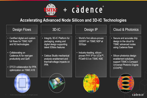
TSMC’s Compact Universal Photonic Engine (COUPE) can be supported by Cadence silicon photonics design enablement solutions to handle the increasing communication problems between these devices.
Additionally, TSMC and Cadence are working together with businesses in the automotive industry. IP creation is increasingly more important for present and future process nodes, such as TSMC N5A and later N3A, as the silicon content in today’s automobile designs is growing.
In order to showcase the precision and scalability provided by Cadence’s front-to-backend chip design flows on the Cloud for TSMC’s advanced process nodes, TSMC and Cadence have also partnered. Through this partnership, clients can use Cadence’s extensive suite of Cloud products to expedite design timelines.
Key Comments
According to Chin-Chi Teng, senior vice president and general manager of the Digital & Signoff Group at Cadence, “We are revolutionizing the future of silicon design with AI-powered EDA software, enabled for TSMC’s latest process technologies. Our ongoing collaboration on innovative solutions for next-generation technologies like TSMC A16 and 3Dblox is paving the way for the AI factories of tomorrow.”
“In collaboration with Cadence, we’ve successfully enabled AI-optimized design flows for TSMC’s N2 technology and are driving advancements in 3D-IC design,” said Dan Kochpatcharin, head of Ecosystem and Alliance Management Division at TSMC. “This marks a significant leap forward in digital and custom solutions, paving the way for the technology innovations that will power the AI infrastructure.”
For Further Info: CLICK HERE | CLICK HERE
