


The 3nm Chip Fab project involves an estimated $17 billion investment, building on TSMC’s prior $12.2 billion commitment for less advanced 6-12nm nodes at the same site.

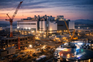
Taiwan Semiconductor Manufacturing Company (TSMC), the world’s leading chip foundry, has announced plans to produce cutting-edge 3nm Chip Fab at its second facility in Kumamoto, southern Japan. This major upgrade responds to surging demand for advanced semiconductors powering AI applications, high-performance computing, and data centers.
Investment and Timeline
The 3nm Chip Fab project involves an estimated $17 billion investment, building on TSMC’s prior $12.2 billion commitment for less advanced 6-12nm nodes at the same site.
Construction of the second fab is already underway, with production technology and timelines adjusted to match customer needs and AI-driven market growth.
Japan’s government, which has subsidized earlier phases, is considering additional funding to support this shift toward state-of-the-art manufacturing.
Leadership Comments
TSMC CEO C.C. Wei confirmed the 3nm strategy during a meeting with Japanese Prime Minister Sanae Takaichi in Tokyo, stating, “We believe this fab will further contribute to the local economic growth and form a foundation for Japan’s AI business.” Wei emphasized ongoing talks with Japanese partners for broader AI ecosystem collaboration, positioning the Kumamoto site as a key diversification move beyond Taiwan.
Strategic Impact
This expansion marks Japan’s entry into domestic 3nm Chip Fab production, vital for economic security and reducing global supply chain risks.
It aligns with Tokyo’s subsidies for TSMC and local player Rapidus, ensuring complementary roles in the semiconductor landscape.
Japan’s TSMC fab is strategically important but still smaller, less advanced (so far), and less profitable than the company’s flagship capacity in Taiwan and its fast-ramping Arizona site.
Process technology and nodes
-
Taiwan (home base): Hosts the bulk of TSMC’s most advanced nodes, including high-volume 3 nm today and 2 nm ramping mid-decade, with multiple fabs dedicated to these processes.
-
Arizona, USA: Fab 21 is in volume production on 4 nm, with a second module planned for 3 nm around 2028 and a third targeting 2 nm/1.6 nm later in the decade.
-
Kumamoto, Japan: First fab focuses mainly on mature/automotive nodes (12/16/22/28 nm), with 3 nm planned through an upgraded second fab, giving Japan its first domestic access to cutting?edge logic but at a smaller scale than Taiwan.
Capacity, cost and economics
-
Taiwan: Massive, dense cluster of fabs; 3 nm monthly capacity alone is expected to exceed 200,000 12-inch wafers by end 2026, making it the cost and scale benchmark.
-
Arizona: Current output is estimated around 10,000 wafer starts per month on 4 nm, with yields reported comparable to Taiwan; however, per chip manufacturing costs in Arizona are higher due to labor and construction costs.
-
Japan: Kumamoto’s two fabs together are projected to exceed 100,000 12-inch wafers per month across nodes, but utilization has been around 50% and the venture posted a net loss of about NT$4.5 billion in H1 2025, reflecting weaker demand and slower adoption of advanced nodes in Japan’s auto sector.
 Strategic role and ecosystem
-
Taiwan: Core of TSMC’s R&D, ecosystem, and supply chain; primary site for each new node’s first high-volume ramp, tightly coupled with global customers like NVIDIA, Apple, and others.
-
Arizona: Geopolitical and customer?driven; central to U.S. CHIPS Act goals and “on-shore” capacity for American customers, helping the U.S. target 20% of global leading-edge logic by 2030.
-
Japan: Security and supply-chain resilience play for Tokyo; heavily subsidized to rebuild Japan’s chip base and support automotive/industrial demand, with 3 nm aimed at anchoring an AI and auto electronics ecosystem in Kyushu.