Producing 2nm node chips isn’t just a matter of scaling components down, explained Dechao Guo, the director of advanced logic technology at IBM Research.
Modern chip architecture is also evolving as the need for more energy-efficient, smaller, and more powerful chips—particularly for AI applications—increases. In order to overcome the technological difficulties posed by transistors’ growing complexity and diminishing footprints, IBM is developing fresh and new approaches to the construction of these devices.
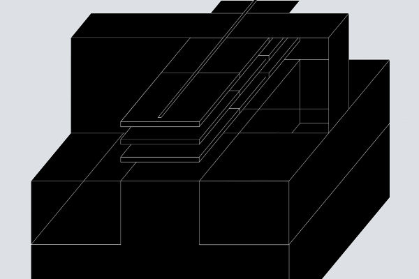
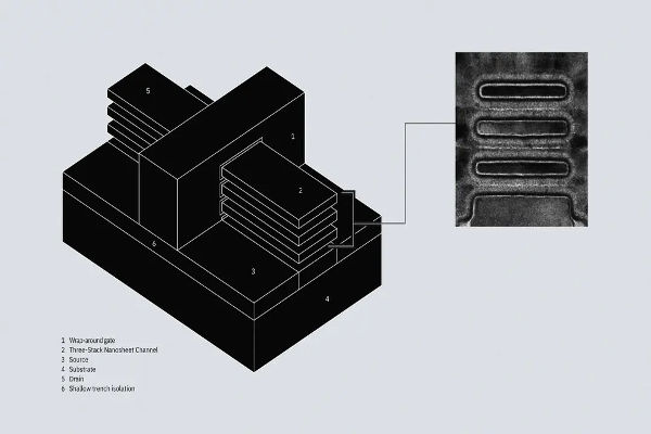
In light of this, researchers from IBM and the Japanese chipmaker Rapidus have said that they have successfully built semiconductors using a 2-nanometer process, marking a significant milestone. They may now construct using two distinct methods for selectively reducing the nanosheet layer. IBM For almost 15 years, research has been at the forefront of gate-all-around transistor technology, driving the development of stacked nanosheets from single nanowires.
More transistors may be accommodated in a given footprint thanks to nanosheets, which also offer superior electrostatic control over nanowires.Multiple threshold voltages (also known as multi-Vt) in nanosheet gate-all-around transistors enable circuits that can carry out intricate calculations with less energy consumption.
The team discovered that they could accomplish this without the metal gate boundary issues that frequently arise with this manufacturing technique. Recently, at the annual IEEE International Electron Devices Meeting (IEDM) in San Francisco, they give a presentation on their latest findings.
The world’s first 2 nanometer node chip was shown by IBM Research scientists three years ago, and two years ago, Rapidus and IBM partnered to develop the technology to the point where 2 nm circuits could be produced on a large scale.
The partnership has made significant progress toward the objective of manufacturing these chips by the end of this decade with their latest findings.

Kazuyuki Tomida, the general manager at Rapidus US, LLC, also mentioned, “Multi-Vt technology is a critical component of our nanosheet architecture. The joint publication of this technology research paper with IBM Research at the IEDM conference represents a substantial milestone for Rapidus. This achievement reinforces our confidence in realizing our goal of manufacturing in Hokkaido at our advanced IIM foundry.”
Diving into the World of 2 nm Node Chips
Producing 2 nm node chips isn’t just a matter of scaling components down, explained Dechao Guo, the director of advanced logic technology at IBM Research. It also introduces unique challenges compared to the previous industry standard, FinFET transistors. “To achieve our goals for 2 nm technology, we need process solutions with nanosheet gate-all-around architecture for multiple threshold voltages, which enable ultra-low threshold voltages for high-performance computing, and higher threshold voltages for low-power computing,” he said.
In a 2017 study, IBM researchers claimed that nanosheets would allow the industry to develop transistors that are even thinner and more effective than FinFET. This building technique allows for the packing of more transistors into a given space by entirely enclosing the transistor gate with thin silicon sheets called nanosheets.
However, it also presented fresh difficulties. A significant step toward the initial version of the upcoming generation of microchips has now been proven by the team.
“Nanosheet is a very different structure compared to the previous generation FinFET, and it can be more complicated” said Ruqiang Bao, senior technical staff member at IBM Research. “The new production process we propose is simpler than the approach used previously, and we’re confident it will make it easier for our partner Rapidus to reliably make chips with 2 nm nanosheet technology at scale.”
“Multi-Vt presents multiple challenges when using nanosheet technology, so we’ve been solving them, one by one,” said Bao. Over the years, they’ve had several achievements. The first two solutions they presented at IEDM in 2019: Tsus pinchoff and volumeless multi-Vt. These solve the issues raised by Tsus for replacement metal gate patterning of materials onto chips. “The material required for multi-Vt is less than 1 nm thick, and the material diffuses into the underlying structure, hence making it essentially volumeless,” said Guo.
The full story can be read here


