


Sarcina Technology’s goal is to further the development of AI computing systems by offering a distinctive platform that makes it possible to create economical, scalable, adaptable, and efficient semiconductor packaging solutions for AI applications.
Sarcina Technology has announced the debut of its new artificial intelligence (AI) platform, which will enable advanced AI packaging solutions that can be customized to satisfy particular customer needs.
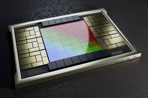
This platform contains an interposer that supports chiplets employing UCIe-A for die-to-die interconnects, utilizing ASE’s FOCoS-CL (Fan-Out Chip-on-Substrate-Chip Last) assembly technology. This enables the implementation of innovative, affordable, and reliable solutions.
Sarcina Technology’s goal is to further the development of AI computing systems by offering a distinctive platform that makes it possible to create economical, scalable, adaptable, and efficient semiconductor packaging solutions for AI applications.
More complex packaging methods that can handle greater processing demands are required as AI workloads continue to develop.
Sarcina’s innovative interposer packaging technology combines high-efficiency interconnects with industry-leading memory solutions. Sarcina’s new AI platform can deliver whether cost, performance, or power efficiency are the top priorities.
Designing high-power, high-performance semiconductor packages is an area in which Sarcina specializes. This eliminates the need for a costly post-silicon design and manufacturing team, allowing semiconductor firms to concentrate on creating effective algorithms for generative AI and edge AI training.
Startups can streamline the process, cut expenses, and maintain good performance by just developing their silicon and sending it to Sarcina for post-silicon packaging.
AI customers can leverage chiplets to create sizable silicon regions with Sarcina’s die-to-die interposer system, enabling high-performance computing with acceptable wafer yields. More memory may be integrated thanks to this large package design, which is essential for generative AI applications that need to process data quickly and in parallel.
In order to achieve data rates of up to 32 GT/s, the Sarcina team has successfully built an interposer with up to 64 bits of data interface per module.
According to the UCIe 2.0 standard, this provides the best UCIe-A performance in terms of both bandwidth and data rate. It is possible to organize several modules in parallel along the silicon die edge to further increase the throughput of data transfer. Additionally, LPDDR5X/6 packaged memory chips and HBMs are available.
Key features of the new Sarcina AI platform:
- Cost-effective chiplet design: A cost-efficient alternative to expensive SoC solutions.
- Fast die-to-die interconnection with UCIe-A standard: Up to 64-bit data interface per module and 32 GT/s transmission speed per lane. Supports multi-module configurations, interconnect redundancy and side-band configurations as specified by UCIe 2.0 standards.
- FOCoS-CL advanced packaging technology: A cost-effective replacement for costly 2.5D TSV (Through-Silicon Via) silicon interposer technology, as well as other expensive solutions like silicon bridge die with fan-out RDL interconnections.
- LPDDR5X/6 and HBM options: Provides superior memory bandwidth and efficiency to support a variety of AI workloads. LPDDR6 memory also incorporates 3D stacking technology similar to HBM, achieving data rates of approximately 10 GT/s.
- Scalable package size: Supports package sizes up to 100 mm x 100 mm, enabling scalability for diverse AI applications.
- Power specifications: <500W for forced air cooling and up to 1000W with liquid cooling, offering flexible deployment options.
- Memory integration: Supports up to 20 LPDDR5X/6 memory chips or up to 8 HBM3E chips, facilitating high-speed data processing for AI workloads.
The launch of Sarcina’s AI platform is set to transform AI computing capabilities across industries such as autonomous systems, data centers and scientific computing.
Sarcina Technology is also a leading provider of silicon photonic semiconductor packaging and testing solutions. Meet the team on booth 3019 at the Optical Fiber Conference (OFC) San Francisco, CA, USA (30 March – 3 April 2025). www.ofcconference.org
Leadership Comments
According to Dr. Larry Zu, CEO of Sarcina Technology:
“Six years ago, after prototyping a 2.5D silicon TSV interposer package that integrated one ASIC and two HBMs, we predicted this technology would enable highly complex compute solutions. Today, this vision is becoming a reality, driven by RDL die-to-die interconnects like UCIe.”
Zu continues: “With FOCoS assembly technology, we are entering a new era of AI computing. Our AI platform offers greater efficiency and customization, with the lowest cost in the industry for generative AI chips. This ensures that our customers stay competitive in the rapidly evolving AI landscape.”
For Further Info: CLICK HERE