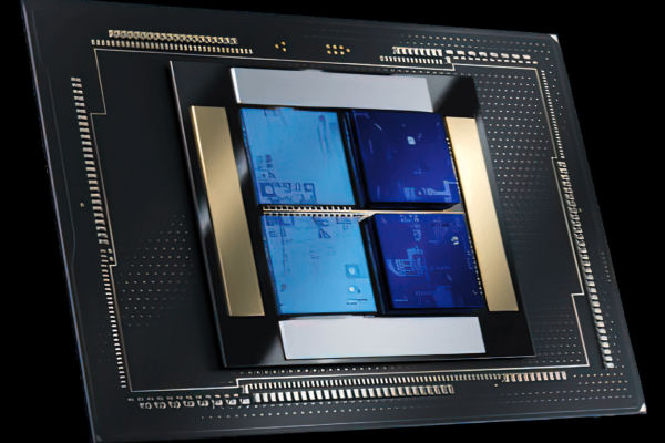
Intel made the unexpected announcement lately that it will no longer be using its indigenous ‘Intel 20A’ process node with its future consumer-oriented Arrow Lake processors. Instead, all of Arrow Lake’s chip components will be sourced from external nodes, most likely from partner TSMC. 
Packing the externally created chiplets into the final processor will be Intel’s only manufacturing duty for the Arrow Lake processors. During the firm’s talk at the Citi Global TMT Conference lately, Intel CFO Dave Zinsser also addressed the issue and said the business would “skip over productizing” the 20A node in order to cut costs and capital expenditures. Intel estimates that omitting the 20A node will save it $500 million.
15,000 Employees Jobs in Danger
The news comes as a wave across the industry as Intel begins a massive reorganization following unsettling financial results from the previous quarter.
15,000 employees are still being let go by the corporation, which is one of the biggest employee reductions in its 56-year existence.
Earlier Hints of Arrow Lake Family Opting TSMC Node
Following Intel’s original demonstration of an Arrow Lake CPU wafer fabbed on the 20A node during its Innovation 2023 event, which suggested the chips were already far advanced in the development cycle, the node was changed. Intel stated at the time that Arrow Lake would launch in 2024. Since then, industry speculations have suggested that a portion of the Arrow Lake family might utilize a TSMC node, with the 20A node being used for the remainder.
‘Intel 18A’ Node is Still Scheduled for 2025?
As per Intel, the release of its highly anticipated next-generation ‘Intel 18A’ node is still scheduled for 2025. The company claims that the strength of the yield metrics for 18A is what motivated them to switch its engineering resources from the older 20A process Node to the more recent 18A node. Once more, Intel reported that for 18A, it had achieved a sub-0.40 D0 defect density (def/cm^2)—a crucial indicator of a process node’s yield rate.
Once D0 falls to 0.5 or less, a process node is often regarded as healthy and ready for production.
With this move, Intel will completely bypass its 20A process and save money on the capital costs needed to get the node up and running. The business will undoubtedly fulfill its cost-cutting targets if the always-appealing ramp charges of a new node—especially one as sophisticated as 20A—are eliminated. Intel estimates that this move will save half a billion dollars.
Race Towards Five Nodes in Four Years
Building out an extensive 20A production would yield limited returns, as the company is racing to reach its target of producing five nodes in four years, and the 20A node was never envisaged for many products. Instead, the company moved quickly to the more advanced 18A node. But Intel’s 20A paved the way for a number of groundbreaking innovations, including the first new Intel technology, RibbonFet Gate-All-Around (GAA) technology.
20A Process Node Helped its Intel 18A Node Succeed
Since Intel 18A is a more precise version of the technologies developed for 20A, Intel claims that the knowledge it acquired from its 20A process Node helped its 18A node succeed. There will inevitably be rumors that Intel’s 20A node had yield problems, but as far as we know, there are no outside signs indicating the 20A process node condition.
Inputs taken from, Tom Hardware


