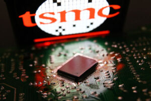
The plan to start mass producing 2nm chips in 2025 is still on track, as TSMC is said to have started trial production of the chips at its Baoshan Plant in Hsinchu, northern Taiwan. The 2nm wafers are anticipated to cost twice as much as 4/5nm wafers, perhaps surpassing USD 30,000 per wafer.
The research points out that TSMC’s market monopoly and strong pricing power are the reasons behind the rising cost of 2nm wafers, despite rumours that the yield rates for Intel and Samsung’s advanced nodes are comparatively low.
The report claims that semiconductor industry sources have stated that fabs have made significant investments in cutting-edge procedures. For example, the R&D investment of $3 billion might surpass $4 billion USD, with important supply chain partners of TSMC, including Taiwanese suppliers of materials and intellectual property, playing a crucial role.
According to executives from IC design firms cited in the article, the R&D expense for advanced nodes remains high even when seen through the lens of IC design.
Development Cost for 28nm
As an illustration, the development cost for 28nm is approximately USD 50 million, whereas the potential expenditure for 16nm might reach USD 100 million. The R&D cost for 5nm has risen to USD 550 million when the costs of software verification, IP licensing, and design architecture are included.
As per the report, foundries have made even greater investments; research institutions estimate that R&D costs for 3nm might be somewhere between USD 4 billion and USD 5 billion.
As a result, the paper points out that for a foundry, developing a new generation of node requires enormous work and requires partners in three important areas: materials, software (including IP and EDA tools), and equipment.
Long-term partnerships are typically secured by suppliers once their goods have been approved by the foundry.
According to the research, the taiwanese semiconductor contract manufacturing and design company major suppliers should experience a tremendous profit increases when 2nm launches in 2025.
The report claims that Taiwanese intellectual property company M31, for instance, has already created intellectual property that supports the 2nm platform for high-performance computing and cellphones. Similarly, eMemory has said that it is working with top foundries to create 2nm.
On the other side, as 2nm technologies require smaller wafers, Taiwan-based materials businesses, such as Kinik and Phoenix Silicon International Corp., have entered the markets of diamond discs and recovered wafers.
The paper states that the market value of recycled wafers at 2nm is around 4.6 times that of 28nm. Furthermore, with sophisticated processes, there will be a rise in the quantity of dummy wafers, which benefits vendors that can offer higher average pricing and greater volume.
Source: Commercial Times


