


TCS’s offering includes advanced package design technologies such as 2.5D and 3D interposers and multi-layer organic substrates.
Tata Consultancy Services (TCS) has announced a major expansion of its semiconductor services portfolio with the launch of chiplet-based system engineering solutions, marking a significant step in accelerating innovation for the global chip industry.
This initiative is positioned to bolster India’s ambitions to become a leading global hub for chip design and manufacturing, as the domestic semiconductor market is expected to surge from $45-50 billion in 2024-2025 to an impressive $100-110 billion by 2030.
Reinforcing India’s Semiconductor Ecosystem
Central to the country’s strategy is the India Semiconductor Mission (ISM), backed by the Union Cabinet with a funding outlay of ?76,000 crore. ISM aims to foster a robust ecosystem spanning chip fabrication, advanced design, and large-scale manufacturing.
India’s prominent position is evidenced by the fact that 20% of the world’s chip design engineers are already based in the country, and global multinational players have continued to invest in manufacturing and assembly facilities here.
TCS’s newly launched services are set to further catalyze this momentum, providing Indian and international companies access to world-class chip-to-system engineering expertise.
Advanced Chiplet Packaging and Design
Tata Consultancy Services offering includes advanced package design technologies such as 2.5D and 3D interposers and multi-layer organic substrates.
These solutions deliver critical enhancements for next-generation chips including greater signal integrity, lower latency, and more compact layouts—essential attributes for the development of multi-chip products that are increasingly vital in high-performance computing, artificial intelligence, and IoT sectors.
Impact on Industry and Global Partnerships
Industry leaders recognize the transformative nature of TCS’s chiplet-based services for global chipmakers. The company’s comprehensive investment in next-gen semiconductor technologies, deep industry insight, and strong execution track record make it an attractive partner for innovation at scale.
As articulated by V Rajanna, President, Technology, Software and Services at TCS, “Our extensive investments in next-gen technologies, contextual knowledge of the semiconductor industry, and strong track record in execution make us the preferred partner to drive innovation at scale.” These services aim to expedite chiplet integration and tape-out, providing unprecedented flexibility, scalability, and efficiency, and reducing time to market for clients worldwide.
Leadership Comment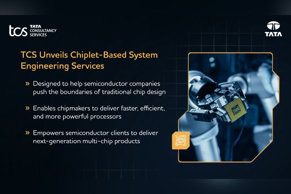
Sanjay Suri, Senior Vice President of Semiconductor Solutions at TCS, commented, “With the launch of chiplet-based system engineering services, TCS reaffirms its commitment to advancing India’s semiconductor capabilities. This is a strategic moment for both our company and the nation, enabling faster commercialization cycles and robust global collaborations that will shape the future of chip innovation.”
Driving Semiconductor Innovation
The recent collaboration between TCS and a North American semiconductor company demonstrates the impact of these services in real-world scenarios. By utilizing chiplet-based methodologies, the partner was able to seamlessly integrate diverse chip types into a unified system, modernizing its design processes and establishing new benchmarks for simplicity and performance.
TCS’s expanded chiplet-based services epitomize India’s rise as a center for advanced semiconductor engineering, promising new paradigms of speed, efficiency, and creativity for chipmakers ready to embrace the opportunities of the next decade.