


A new high-volume 200mm SiC production facility for test and packaging, power devices, and modules is set to be constructed in Catania, Italy, according to STMicroelectronics.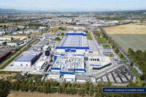
ST’s objective of a completely vertically integrated manufacturing facility for the mass production of SiC on one site will be realized when these facilities are combined with the SiC substrate manufacturing facility that is being prepared on the same location to establish ST’s Silicon Carbide Campus affirmed its official release.
An important step in assisting clients using SiC devices in cloud infrastructure, industrial, and automotive applications as they move toward electrification and increased efficiency is the establishment of the new Silicon Carbide 200mm silicon carbide (“SiC”) production facility.
“The fully integrated capabilities unlocked by the Silicon Carbide Campus in Catania will contribute significantly to ST’s SiC technology leadership for automotive and industrial customers through the next decades,” said Jean-Marc Chery, President and Chief Executive Officer of STMicroelectronics. “The scale and synergies offered by this project will enable us to better innovate with high-volume manufacturing capacity, to the benefit of our European and global customers as they transition to electrification and seek more energy efficient solutions to meet their decarbonization goals.”
Acting as the hub of Silicon Technologies’ worldwide SiC ecosystem for ST, the Silicon Carbide Campus will integrate every stage of the production flow, including the development of SiC substrates, epitaxial growth processes, 200mm front-end wafer fabrication, and back-end assembly of modules.
It will also facilitate process research and development, product design, and state-of-the-art die, power system, and module R&D and packaging capabilities. By leveraging 200 mm technologies for improved yields and performances, this will result in the first-ever mass production of 200 mm SiC wafers in Europe at every stage of the process, including substrate, epitaxy & front-end, and back-end.
It is planned for the 200mm SiC production facility to begin production in 2026 and reach maximum capacity by 2033, producing up to 15,000 wafers per week when fully built out. It is anticipated that the investment would reach around five billion euros, with the State of Italy contributing an additional two billion euros in assistance under the EU Chips Act.
The Silicon Carbide Campus, 200mm SiC production facility is designed, developed, and run using sustainable principles to guarantee responsible use of resources, such as electricity and water.
What is a Silicon Carbide (“SiC”)?
For power applications, silicon carbide, or “SiC,” is a crucial compound material (and technology) made of silicon and carbon.
It has a number of benefits over traditional silicon. SiC’s broad bandgap and inherent qualities, such as improved thermal conductivity, faster switching speeds, and lower dissipation, make it ideal for high-voltage power device production (especially above 1,200V).
Fostering SiC Legacy Further
With a sizable portfolio of important patents and 25 years of dedication to research and development, ST has become a pioneer in the SiC industry. Being the location of the largest SiC R&D and production activities, Catania has long been a hub for innovation for ST and has effectively contributed to the development of innovative ways for generating more and better SiC devices.
With a well-established power electronics ecosystem, a vast network of suppliers, and a successful partnership between ST and the University of Catania and the CNR (Italian National Research Council), Catania will be better positioned to grow and become a global hub for SiC technology thanks to this investment.
ST’s Two 150-millimeter Wafer Lines in Catania, Italy, and Ang Mo Kio, Singapore
Currently, ST uses two 150-millimeter wafer lines in Catania, Italy, and Ang Mo Kio, Singapore, to produce its signature high-volume SiC products. A third hub, a joint venture with Sanan Optoelectronics, is being built in Chongqing, China, and will service the Chinese market with a 200-millimeter facility devoted to ST.
Automotive-qualified, high-volume assembly and test operations in Bouskoura, Morocco, and Shenzhen, China, complement ST’s wafer manufacturing facilities.
The majority of ST’s R&D and design team for SiC products are headquartered in Catania, where the company is expanding its production, and Norrköping, Sweden, is the site of SiC substrate R&D and industrialization.