


China scientists demo damage-free ‘self-etching’ for 2D perovskites, paving the way for ultra-fine, full-color optoelectronic pixels on atomically thin wafers.
![]()
Breakthrough in gentle perovskite processing
An international team from the University of Science and Technology of China, Purdue University and ShanghaiTech University has unveiled a guided “self-etching” process for soft ionic-lattice semiconductors such as 2D perovskite thin-layer single crystals.
Instead of using aggressive solvents or UV patterning, the method exploits internal stress built up during crystal growth and a mild ligand–isopropyl alcohol (IPA) solution to trigger controlled in-plane etching only at predefined sites.
How the self-etching heterojunctions work
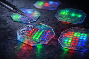
Once the self-etching forms nanoscale cavities, the researchers refill these voids with 2D perovskites having different halogen compositions, forming seamless heterojunctions inside a single crystal wafer.
The result is lattice-continuous, atomically smooth interfaces that allow precise tuning of emission color and brightness in each cavity, effectively creating pixel-like light-emitting units on an ultrathin chip.
Advantages over conventional etching
Traditional patterning routes for perovskites, such as strong solvent treatments, photolithography or UV patterning, often roughen or partially destroy the fragile crystal lattice and degrade device performance.
By contrast, the guided self-etching strategy is significantly gentler, maintaining structural integrity while still enabling high-resolution feature definition required for next?generation photonics and displays.
 Key Comments
Members of the research collaboration describe the technique as a new materials and design platform for future high-performance luminescent and display technologies.
“This processing method suggests that in the future, we may integrate densely arranged microscopic light-emitting pixels of different colors on an ultra-thin material, opening a new pathway for compact, energy-efficient display and optoelectronic devices,” noted Zhang Shuchen from the team.
Source: Xinhua News Agency